Table of Contents
A prototype that cannot be manufactured at scale is a business failure. This is a lesson many engineering teams learn too late in the product lifecycle. Effective PCB design for manufacturing (DFM) is not a final checklist before sending Gerber files to a fabricator; it is a core strategy that bridges the gap between a validated concept and a profitable, reliable product.
Integrating manufacturability into the design process from the outset mitigates costly respins, compresses time-to-market, and significantly lowers production risk.
Why Design for Manufacturing Is Non-Negotiable
A common failure mode for hardware projects is the late discovery of manufacturability issues. Teams invest significant resources into a functional prototype, only to find the design is incompatible with their contract manufacturer’s (CM) volume production processes. This leads to poor yields, excessive costs, or, in the worst cases, a complete redesign.
This reactive approach treats DFM as a final validation step rather than a continuous engineering discipline. The problem often stems from a disconnect: engineers, focused on performance and features, may inadvertently specify component clearances, via structures, or materials that are difficult or impossible to produce consistently at volume.

The solution is to integrate DFM into the entire product development lifecycle. Engage manufacturing partners early to understand their specific capabilities and constraints. Design decisions must balance performance targets with production realities. For a deeper analysis of this integrated approach, see our guide on Design for Manufacture and Assembly.
The business impact of this strategic alignment is substantial:
- Risk Reduction: Early identification of potential fabrication or assembly failures prevents expensive post-production fixes and mitigates the risk of product recalls.
- Cost Control: Designing for existing manufacturing processes reduces tooling costs, material waste, and the need for manual intervention during assembly.
- Speed to Market: Eliminating board respins and production holds creates a more predictable and accelerated path from prototype to full-scale production.
This strategic approach is increasingly critical. The global printed circuit board assembly market is projected to reach approximately $88.1 billion by 2030. This growth is driven by demanding sectors like aerospace and medical devices, which require sophisticated DFM to manage advanced technologies like high-density interconnect (HDI) PCBs while meeting stringent requirements for miniaturization and reliability.
Real-World DFM Scenario: Medical Device Thermal Management
A medical device company developed a portable diagnostic tool with a dense, high-power PCB intended for a sealed enclosure. The prototype functioned correctly in a lab environment. However, the design team had not adequately considered the thermal management constraints of mass production, a critical factor for compliance with the ISO 13485 quality standard.
- Problem: The layout concentrated high-power components in a single area with inadequate thermal dissipation pathways. In real-world operation, this would lead to overheating and premature component failure.
- Diagnosis: A pre-production DFM review with the selected CM immediately flagged the thermal risk. The CM’s thermal simulations predicted that operating temperatures would exceed component specifications, leading to device failures and a probable product recall.
- Solution: The design team collaborated with the CM to revise the PCB layout. High-power components were distributed more evenly, an array of thermal vias was added under the main processor to sink heat to an internal ground plane, and a thicker copper weight was specified for improved heat spreading. These were minor layout modifications that did not alter the device form factor.
- Outcome: By addressing the thermal management issue during the design phase, the company avoided catastrophic field failures. The final product was more reliable, fully compliant with regulatory standards, and launched on schedule, securing its market position and ensuring patient safety. This demonstrates the direct business value of proactive DFM.
Aligning Your Design With Fabrication Realities
A PCB design is only as good as the contract manufacturer’s ability to build it reliably and at scale. A design that appears optimal in an EDA tool can become a low-yield, high-cost liability if it ignores the physical constraints of the production floor.
Success requires treating fabrication and assembly rules not as a final checklist, but as foundational design parameters. This involves navigating a series of critical tradeoffs where every choice directly impacts cost, density, signal integrity, and overall project risk.
Navigating Key DFM Tradeoffs
Every design decision involves balancing competing constraints. Consider the choice between standard through-hole vias and laser-drilled microvias, which has significant downstream consequences.
Standard Vias: Mechanically drilled and inexpensive, these are the industry workhorse. However, their larger size consumes valuable routing real estate, limiting board density. A high aspect ratio (board thickness vs. drill diameter) complicates reliable copper plating within the via barrel, creating a risk of open circuits.
Microvias: For High-Density Interconnect (HDI) designs, microvias are essential for BGA fanout (e.g., 0.4 mm pitch BGAs) and can dramatically increase routing density. The tradeoff is increased cost and manufacturing complexity. Microvias require specialized laser drilling equipment and add lamination cycles to the fabrication process, which can impact yield at less capable facilities.
Real-World Scenario: An industrial IoT team needed to reduce their product’s form factor by 30%. Their initial design used standard vias but could not route out from a dense BGA processor without adding layers, which would have exceeded their cost target.
- Problem: The primary constraint was not trace width, but the large via pads consuming routing channels.
- Solution: The design was revised to use a stacked microvia structure, an HDI technique that allows for via-in-pad placement.
- Outcome: This freed critical routing channels on the outer layers, enabling the team to meet the size target without adding layers. The marginal increase in board cost was significantly less than the cost of a larger, custom-molded enclosure.
The table below outlines common tradeoffs and their impact on fabrication and assembly.
Key DFM Tradeoffs: Fabrication vs. Assembly
| Design Decision | Fabrication Impact (Cost/Yield) | Assembly Impact (Yield/Reliability) | Recommendation |
|---|---|---|---|
| Microvias vs. Through-Hole Vias | Microvias significantly increase fab cost (laser drilling, extra lamination cycles) but enable higher density. | Via-in-pad with microvias can simplify BGA escape routing but requires a planarized, filled via to prevent solder wicking, which adds an assembly step/cost. | Use standard vias unless density absolutely requires HDI. If using microvias, discuss via filling/capping requirements with your assembler early. |
| Trace/Space Reduction | Tighter traces/spaces (e.g., 3/3 mil vs. 5/5 mil) push fab capabilities, increasing cost and potentially lowering yield due to shorts/opens. | Tighter spacing between pads (e.g., on QFNs) increases the risk of solder bridging during reflow. | Adhere to your CM’s standard or “Class 2” capabilities unless necessary. For fine-pitch parts, confirm solder mask web capabilities with the assembler. |
| Material Choice (e.g., FR-4 vs. Rogers) | High-frequency materials like Rogers are more expensive and may require specialized processing, increasing fab cost and lead time. | Material properties (CTE) can affect solder joint reliability over thermal cycling, especially with large components. | Use standard FR-4 unless your signal integrity requirements (RF, high-speed digital) mandate a specific high-performance material. |
| Panelization Scheme | An inefficient panel layout wastes material, driving up the per-board cost. Complex outlines or breakaway tabs can reduce yield. | Poorly designed breakaway tabs (“mouse bites”) can leave rough edges, cause delamination, or make depaneling difficult, potentially damaging boards or components. | Collaborate with your CM on the panel layout. Use V-scores for straight edges and well-placed mouse bites with perforations for irregular shapes. |
A decision that saves cents in fabrication can cost dollars in assembly yield loss or field failures. An integrated view is essential.
Preventing Common Production Failures
Many costly production issues originate from seemingly minor layout choices. Proactive pcb design for manufacturing involves identifying and eliminating these problems before design release.
- Acid Traps: Acute angles in copper traces can trap etching solution during fabrication, leading to over-etching. This creates a latent defect—an open circuit or weak point that may fail in the field. Solution: Route all trace corners at 45° angles or with curves. Avoid 90° or sharper angles. Most EDA tools include design rules to enforce this.
- Tombstoning: A passive component (e.g., an 0201 resistor) lifts at one end during reflow soldering. Cause: Imbalanced thermal mass between the two pads. One pad connected to a large copper plane dissipates heat, while the other pad on a thin trace heats quickly. Solder on the hotter pad melts first, and surface tension pulls the component up. Solution: Use thermal relief pads to connect component pads to large copper planes, ensuring both pads heat at a similar rate.
- Solder Bridging: Excess solder flows between adjacent component pads, creating an electrical short. This is a common failure mode with fine-pitch components. Solution: Ensure the solder mask “web” (the sliver of mask between pads) is wide enough for your CM’s process. For very fine-pitch components where a web is not possible, specify “solder mask defined” pads, where the mask opening defines the solderable area.
Designing for Global Supply Chain Resilience
Your choice of manufacturing partner directly impacts design constraints. While the Asia-Pacific region dominates the PCB assembly market forecast, relying on a single source or region introduces significant supply chain risk. For North American and European companies, understanding regional manufacturing capabilities is critical as reshoring incentives and tariffs alter the cost equation.
This necessitates a strategic choice:
- Design for a Specific CM: Tightly coupling a design to one manufacturer’s most advanced capabilities can optimize cost and performance for high-volume production. The risk is vendor lock-in.
- Design for Portability: Adhering to more common, widely available process rules ensures the design can be moved to another supplier with minimal friction. This builds resilience at the potential cost of ultimate optimization.
For most mission-critical or regulated applications, designing for portability is the more prudent long-term strategy, as it reduces dependency and provides flexibility in a volatile supply chain environment.
Choosing Materials and Designing a Robust Stackup
The selection of materials and the layer stackup form the foundation of a reliable, manufacturable PCB. Selecting a laminate based solely on electrical properties from a datasheet can lead to delamination, impedance variations, or excessive warpage during production.
Effective pcb design for manufacturing requires co-designing the stackup with your fabricator. Provide them with your performance requirements—impedance targets, dielectric constant (Dk), and loss tangent (Df)—and allow them to propose a specific material set and layer construction they can produce consistently.
This collaborative approach mitigates significant risks. Fabricators typically stock specific prepreg and core thicknesses. Designing around their inventory can reduce lead times and material costs.
The Critical Role of Material Properties
Beyond electrical specifications, the mechanical and thermal properties of materials directly impact long-term reliability. The Coefficient of Thermal Expansion (CTE) is a critical parameter, especially for multilayer boards with dissimilar materials or products operating in harsh environments.
A CTE mismatch between the laminate, copper, and components creates mechanical stress during thermal cycling. This stress is a common cause of latent field failures, including:
- Pad Cratering: The component pad delaminates from the PCB substrate.
- Via Barrel Fatigue: Plated through-holes crack, creating intermittent open circuits.
- Solder Joint Failure: Repeated stress cycles lead to solder joint fractures.
Regulatory compliance also influences material selection. European regulations like the REACH Directive SVHC list require validation of the chemical safety of all product components, adding complexity to material choices.
Real-World Use Case: Aerospace Vibration and DO-178C
An avionics module subject to extreme vibration and wide temperature swings required a dense, 12-layer board with several large BGA components. The project was governed by the DO-178C standard for software in airborne systems, which mandates rigorous reliability and failure analysis.
- Problem: The initial design specified a standard FR-4 variant. While electrically sufficient, the CTE mismatch between the large ceramic BGAs and the PCB laminate was a significant reliability concern.
- Diagnosis: Finite Element Analysis (FEA) was used to model the thermomechanical stress. The simulation predicted that stress on the BGA solder joints under the specified operating temperature range would exceed IPC standards for high-reliability products, indicating a high probability of premature field failures.
- Solution: In consultation with the fabricator, a high-Tg, low-CTE laminate was selected. This material provided a much closer CTE match to the ceramic components, drastically reducing stress. Non-conductive via fill (epoxy-filled and capped) was specified under the BGA pads to improve surface planarity and strengthen the physical connection.
- Outcome: The redesigned board passed all vibration and thermal shock qualification tests. The FEA simulation data became a critical artifact in the DO-178C certification package, demonstrating proactive identification and mitigation of a potential failure mode. This ensured product reliability and averted a costly, schedule-impacting redesign.
Documenting Your Controlled Impedance Stackup
For designs with high-speed signals, precise documentation of the controlled impedance stackup is non-negotiable. Ambiguity is a leading cause of board respins.
Your stackup drawing is a contract with your fabricator. It must specify impedance targets, trace widths, spacings, and reference planes for each controlled line. Including a table that explicitly links signal nets to their required impedance values eliminates guesswork for the fabricator’s CAM engineers.
For every controlled impedance layer, specify:
- Target Impedance: e.g., 50Ω single-ended or 100Ω differential.
- Tolerance: Typically ±10%, but may be tighter for sensitive RF circuits.
- Trace Geometry: The target trace width and spacing.
- Reference Planes: The specific adjacent planes the signal is referencing.
Finally, always request a Time Domain Reflectometry (TDR) test coupon with your order. This sample from your production panel is tested by the fabricator to verify that the manufactured impedance is within your specified tolerance, providing objective proof that the board was built to spec.
Optimizing Panelization for Automated Assembly
Panelization—how individual PCBs are arranged on a larger production panel—is an often-overlooked aspect of pcb design for manufacturing. This decision directly impacts material cost, assembly throughput, and long-term board reliability. A layout that ignores the constraints of automated assembly can create a cascade of downstream problems, increasing costs and reducing yields.
The objective is not just to design a functional board, but to design a board that flows efficiently through a high-speed, automated production line.
Depaneling Methods: The Tradeoffs
The method for separating individual boards from the panel—depaneling—influences component stress and final board quality. The two primary methods are V-scoring and routing with breakaway tabs.
V-Scoring (V-Cut): The fabricator cuts a shallow, V-shaped groove along the top and bottom of the panel where boards meet. It is fast, inexpensive, and leaves a clean, straight edge. However, it only works for straight-line separations and imparts significant mechanical stress on the board during breakout. This stress can damage sensitive components like ceramic capacitors if they are placed too close to the edge.
Routing with Breakaway Tabs (Mouse Bites): For boards with irregular shapes, routing is necessary. Boards are cut out by a routed channel but held in place by small tabs with perforated holes (“mouse bites”). While flexible, this method leaves rough nubs on the board edge that may require secondary finishing operations. Improperly placed tabs can concentrate stress on sensitive areas.
Real-World Scenario: A team designing a small wearable device placed a rigid ceramic antenna less than 1mm from the board edge and specified V-scoring for panelization to minimize cost.
- Problem: First production run yields dropped by over 15% due to inconsistent RF performance.
- Diagnosis: Microscopic inspection revealed hairline fractures in the ceramic antennas. The shock and flexing from snapping the V-scored panels was sufficient to crack these brittle components.
- Solution: The panel was redesigned to use routing. Breakaway tabs were carefully placed away from sensitive components, and a “depaneling stress relief” route was added near the antenna to further isolate it.
- Outcome: Yields returned to nominal levels. The minor increase in per-panel cost from routing was insignificant compared to the cost of scrapped boards and potential field failures.
Fiducials and Tooling Holes: The Keys to Automation
Automated pick-and-place machines rely on vision systems that require reliable reference points. These are fiducial marks—small, circular copper pads with an opening in the solder mask. Without well-defined fiducials, the machine cannot accurately place components, leading to yield loss.
Two types are required:
- Global Fiducials: Typically three marks placed on the panel’s tooling rails (the disposable border). These allow the machine to orient the entire panel and correct for rotational skew.
- Local Fiducials: At least two marks on diagonally opposite corners of each individual PCB within the panel. These provide the fine-grained accuracy needed for precise component placement on that specific board.
In addition to fiducials, tooling holes are non-plated holes on the panel rails used to align the panel on conveyor systems and lock it into fixtures. The standard is three holes, with one offset to prevent incorrect loading.
Consult your CM for their specific requirements for fiducial size, shape, and placement, as well as tooling hole diameter and location. This early communication prevents costly production line stoppages.
Weaving Testability Into Your Design Process
A board that cannot be tested is a business liability. Integrating Design for Test (DFT) and Design for Inspection (DFI) is a core component of a professional pcb design for manufacturing strategy. When testability is an afterthought, designs become difficult to validate, leading to shipment of faulty units and costly field returns.
A common failure is a board that is electronically sound but physically untestable. Layout choices can block critical test points, obstruct the view of Automated Optical Inspection (AOI) systems, or prevent X-ray inspection of BGA packages. This leads to high NDF (No Defect Found) rates, where returned field failures cannot be diagnosed because technicians lack adequate test access.
Strategic Placement of Test Points and Probes
DFT provides electrical access to the circuit for validation and programming. This requires strategically placing test points for spring-loaded probes.
- Component Clearances: In-Circuit Testers (ICT) use “bed of nails” fixtures. Pogo pins require both surface and vertical clearance. Placing a test point next to a tall component like an electrolytic capacitor or heatsink will prevent probe contact.
- Probe Density and Pad Size: Test points should be at least 1.27mm (50 mils) in diameter. Maintain at least 2.54mm (100 mils) center-to-center spacing between points to prevent probes from shorting.
- Distribution: Distribute test points evenly across the board to prevent uneven pressure from the test fixture, which can cause the PCB to bow and lead to unreliable probe contact.
For mission-critical systems, placing test points on the bottom side of the PCB is a best practice. It allows for a single, less complex fixture and keeps the top side clear for components and labels.
Leveraging Boundary Scan for Complex ICs
For dense boards with fine-pitch BGAs, physical test access to every pin is often impossible. Boundary scan (JTAG) provides a solution.
Standardized under IEEE 1149.1, boundary scan integrates test circuitry into the ICs themselves. By connecting these ICs in a “scan chain,” the connections between them can be tested electrically without physical probes. This is a powerful method for detecting shorts, opens, and other assembly defects that would otherwise be invisible. Implementing this requires a dedicated JTAG header and careful routing of the TDI, TDO, TCK, and TMS signals. The embedded systems team will also use this port for programming and debugging, as is common in our firmware engineering services.
Real-World Scenario: Industrial Automation Controller
A client developing an industrial automation controller faced a significant bottleneck in final testing. Each unit required manual connection to a complex test rig for firmware flashing and calibration, a process taking nearly 20 minutes per board.
- Problem: The original design lacked dedicated test or programming points. Technicians used fragile, temporary clips on component leads, a slow and unreliable process that often damaged boards.
- Diagnosis: A DFM review identified the lack of test access as the primary bottleneck. The manual process was unscalable and introduced significant risk of human error.
- Solution: The next board revision included a dedicated array of test pads exposing the programming interface, key analog signals, and power rails. A simple pogo-pin fixture was designed to make all connections in a single action.
- Outcome: The new fixture-based process reduced testing and configuration time from 20 minutes to under 12 minutes—a 40% reduction. This immediately increased production throughput, improved test reliability, and simplified future firmware updates.
Putting DFM to Work: A Practical Framework
Moving from theory to practice requires integrating manufacturing checks into the existing design workflow. This framework organizes critical steps by design stage: schematic, layout, and documentation release.
The single most critical action is to establish a collaborative feedback loop with your contract manufacturer (CM) early in the design process. This transforms DFM from a final gate into an iterative process that reduces risk and accelerates time-to-market.
From Schematic to Layout
During the schematic phase, focus on component selection and library validation. Select components with readily available footprints and package types that align with your CM’s assembly capabilities.
For example, a BGA package offers high density but requires X-ray inspection capabilities that not all assemblers possess. Selecting this package without consulting your CM can lead to costly late-stage changes.
During layout, focus shifts to physical implementation. Decisions regarding trace widths, clearances, via structures, and panelization have direct consequences on production yield and final cost. This diagram illustrates how testability, a core DFM principle, should be integrated from the start.
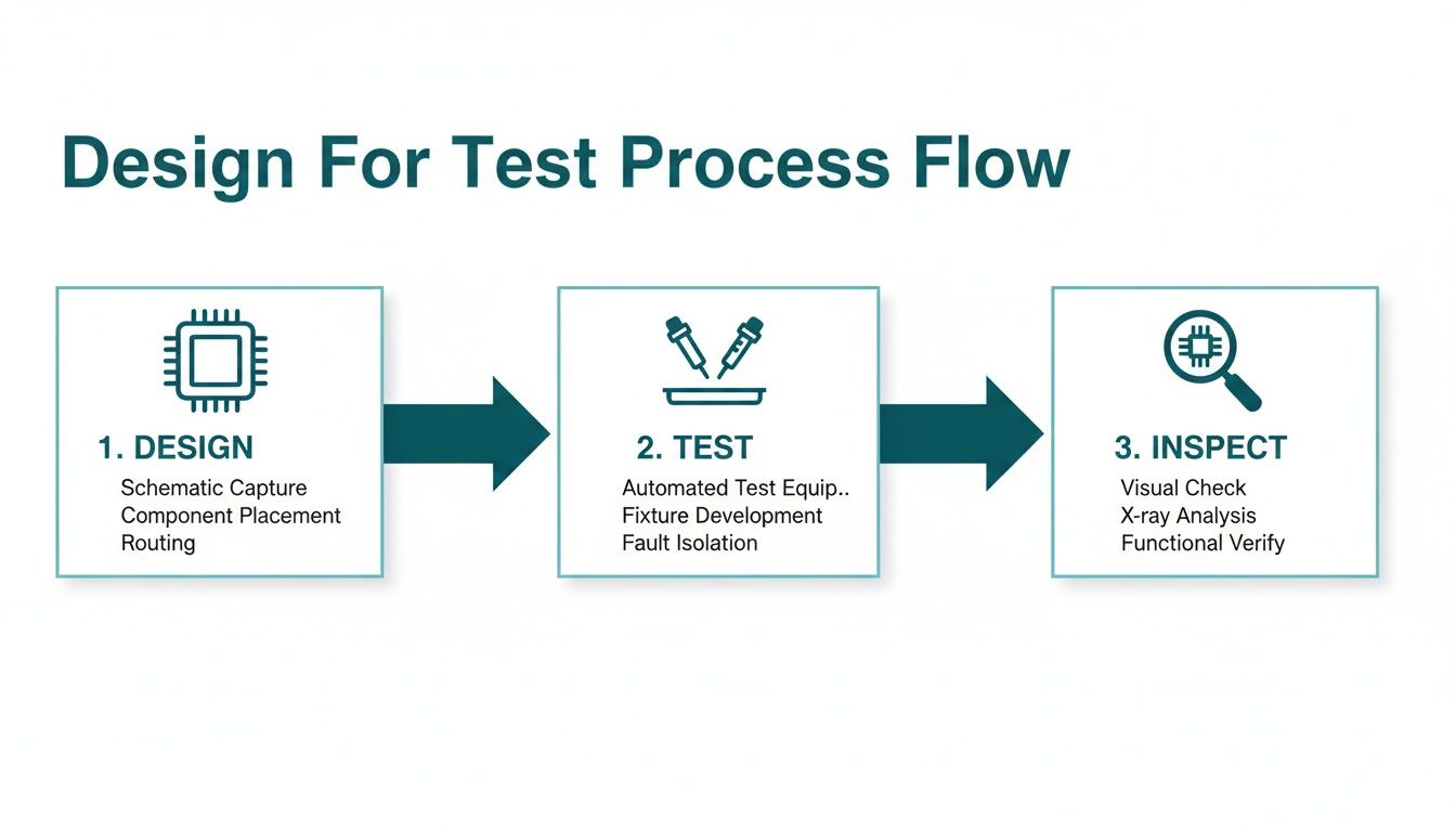
As shown, test and inspection are not afterthoughts but parallel considerations that must influence the PCB layout from its inception.
Documentation and Release
The documentation package is the contract between you and your manufacturer. It must be unambiguous.
- Fabrication Notes: Explicitly specify the layer stackup, material types (e.g., FR-4 TG170), controlled impedance requirements, and any special processes like via filling or plugging.
- Assembly Drawings: Detail component placements, polarity markings (especially for diodes and capacitors), and any specific handling instructions for sensitive components.
- Gerber and Drill Files: Verify that files are generated using the correct formats and units (e.g., 2:5 imperial is a common standard).
This level of detailed documentation is a cornerstone of successful pcb design for manufacturing. Our end-to-end hardware engineering services are built around this meticulous approach to minimize production errors and ensure the design is built exactly as intended.
Burning Questions About PCB DFM
Here are answers to common questions from engineers and project leads implementing a DFM strategy.
When Should I Even Start Thinking About DFM?
DFM should begin at the component selection and schematic capture stage. Early decisions—such as choosing a BGA over a QFP or selecting a specific laminate—have downstream effects on cost, yield, and schedule. The most costly mistakes are those identified after the layout is complete.
A best practice is to engage your contract manufacturer for a preliminary review before starting board routing. This conversation can prevent you from designing into a manufacturability corner.
Won’t a DFM Review Just Slow Down My Schedule?
A proactive DFM review may add a few days of feedback at the beginning of the layout process. However, this initial time investment typically saves weeks or months of delays caused by board respins, production holds, or last-minute component sourcing issues.
The net effect of proper DFM is not a project delay but an acceleration of time-to-market by designing out predictable problems before they can impact the schedule.
What’s The Single Biggest DFM Mistake You See?
Designing in isolation. Teams often follow generic design rules within their EDA software and complete the entire layout before engaging a fabricator.
Every manufacturer has unique equipment, process capabilities, and material stock. A design that is optimal for one facility may be a low-yield, high-cost challenge for another. This creates a significant point of failure.
Early and frequent communication with manufacturing partners is the only reliable way to ensure a design is manufacturable from the outset.
A robust DFM process is the foundation for achieving first-pass success. At Sheridan Technologies, we integrate manufacturability into every project, reducing risk and accelerating the path to production. If your team is facing manufacturing challenges or wants to ensure a smooth transition to volume production for your next project, an initial consultation can identify key risks and opportunities. Learn more about our approach at https://sheridantech.io.