
Table of Contents
Effective circuit board testing is a disciplined process that moves methodically from static checks to a controlled power-up and full functional verification. For experienced engineers, this isn’t about ad-hoc probing; it’s a core risk mitigation strategy. A formal test plan is the critical tool that separates a successful product launch from one plagued by mysterious field failures, costly rework, and schedule overruns. This guide outlines a structured approach to catch problems early, control costs, and ship reliable hardware.
Why a Structured PCB Test Plan Is a Business Imperative

For engineering leaders, circuit board testing is far more than a QA step—it’s a direct control on project risk and budget. An undisciplined, “just wing it” approach to board bring-up introduces a level of variability that can derail a project. The primary danger of unstructured testing is its failure to catch subtle manufacturing defects or design flaws early, which become exponentially harder and more expensive to diagnose once firmware is integrated.
The Business Impact of Ad-Hoc Testing
An informal test process creates quantifiable business risks. Every issue that slips through to a later stage multiplies the cost and schedule impact.
- Skyrocketing Rework Costs: Diagnosing a solder bridge under a BGA after firmware is loaded is a nightmare. It requires depopulating components, expensive rework, and restarting the entire test cycle—a loop that can burn thousands of dollars and weeks of schedule per board.
- Time-to-Market Delays: Each unplanned debug cycle pushes the launch date, giving competitors an advantage and delaying revenue generation.
- Destroyed Product Reliability: Defects missed during prototyping inevitably surface as field failures. This leads to warranty claims, product recalls, and significant brand damage, especially in regulated industries where failure is not an option.
The solution is a phased, documented methodology that treats testing as an integral part of the development lifecycle. This structured approach, central to our process at Sheridan Technologies, transforms testing from a project bottleneck into a development accelerator. To ensure repeatability, it’s vital to create clear Standard Operating Procedures (SOPs) that formalize the entire testing workflow.
A formal test plan is the bridge between a prototype that “works on the bench” and a product that can be manufactured reliably at scale. It forces the engineering discipline required to identify and resolve issues systematically, ensuring predictable outcomes.
From Prototype to Production: A Phased Approach
A robust test strategy evolves with the product’s maturity. The validation goals for a first-run prototype are fundamentally different from the screening requirements of high-volume production.
- Prototype Phase (Design Verification): The focus is on fundamental design validation. Does the architecture work? Are power rails stable? Can core components be accessed? This stage is hands-on, involving manual probing, oscilloscope measurements, and iterative debugging to confirm the design’s integrity.
- EVT/DVT Phase (Design Validation): As the design solidifies, testing shifts to validation against specific product requirements. The objective is to identify process weaknesses and characterize performance. Semi-automated test scripts and fixtures are developed here to ensure repeatable measurements and gather performance data across a larger batch of boards.
- Production Phase (Manufacturing Screening): The goal is high-yield manufacturing screening. Testing must be fast, fully automated, and deliver a definitive pass/fail result. This typically involves dedicated test jigs for in-circuit testing (ICT) or functional circuit testing (FCT) that minimize operator intervention.
This phased approach allows teams to methodically de-risk a new product introduction, resulting in a faster time-to-market, higher first-pass yields, and the product reliability demanded in sectors governed by standards like FDA 21 CFR 820 (medical devices) or AS9100 (aerospace).
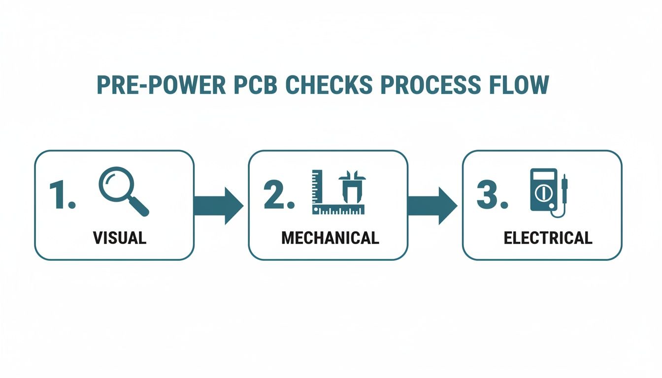
Pre-Power Inspection and Static Checks
Before connecting a power supply, a critical phase of non-destructive checks can prevent catastrophic failure. The moment of first power-on is the riskiest event in a new board’s lifecycle. A disciplined pre-power check is the single best tool for managing that risk by finding manufacturing defects—incorrect components, poor soldering, or mechanical conflicts—before they can cause electrical damage. Rushing this stage is a false economy that often leads to avoidable and time-consuming rework.
Advanced Visual and Mechanical Inspection
A professional visual inspection is a systematic search for subtle defects and requires magnification.
- Component Verification: Double-check the orientation of all polarized components, including diodes, tantalum capacitors, and electrolytic capacitors. A reversed polarized capacitor can fail violently upon power-up, potentially destroying adjacent components.
- Solder Joint Quality: Using a microscope, meticulously inspect solder joints for bridging, cold joints, and insufficient solder, paying close attention to fine-pitch ICs and dense connectors. For components like Ball Grid Arrays (BGAs), where joints are not visible, an X-ray inspection is the only reliable method to verify the absence of hidden shorts or open circuits.
- Mechanical Integrity: Check for physical interference between components, heatsinks, and enclosures. Ensure standoffs are correctly placed and the board does not flex when installed, as mechanical stress can lead to latent solder joint failures.
Real-World Scenario: During the bring-up of a high-power industrial controller, a standard pre-power inspection caught a reversed 470µF electrolytic capacitor in the main DC input filter. Had we powered it on, the capacitor would have likely vented, destroying a $75 power management IC and spraying corrosive electrolyte across the board. The outcome was a five-minute fix instead of a multi-week delay and significant replacement costs.
Essential Static Electrical Tests
With visual and mechanical checks complete, static electrical tests confirm the assembly’s basic integrity without risk. The objective is to find expected connections (continuity) and unexpected ones (shorts). A digital multimeter (DMM) is the primary tool. Knowing how to test continuity with a multimeter is a core skill for this phase.
This workflow is designed to diagnose common assembly mistakes before they become expensive electrical failures:
- Continuity Checks: Methodically probe from key test points to their corresponding component pins to confirm via integrity and that critical signal paths (e.g., JTAG chains, sensor inputs) are fully connected.
- Short Circuit Checks: Test the resistance between every major power rail (VCC, 3.3V, 5V) and ground. A healthy, unpowered board should show very high resistance. A near-zero ohm reading indicates a direct short—likely from a solder bridge or a failed component—that must be rectified before power-up.
- Insulation Resistance Testing: For high-voltage boards (typically >60V), a simple multimeter check is insufficient. A megohmmeter (“megger”) must be used to perform an insulation test between high-voltage planes and the chassis ground. This test applies a high voltage at a very low, safe current to uncover subtle insulation weaknesses or contamination that could lead to arcing or breakdown under load, a critical step for industrial and medical hardware safety.
Mastering the Controlled Power-Up Sequence
Applying power is the moment of truth. A professional, controlled power-up sequence transforms this high-stakes event into a systematic, data-driven diagnostic process. Using a current-limited lab power supply is non-negotiable for any serious board bring-up. Without it, a hidden short circuit on a board powered by an unregulated supply will draw maximum current, often leading to a cascade of failures that can vaporize traces or destroy multiple ICs. A methodical approach isolates faults to specific power domains, gathering diagnostic data instead of creating damage.
Before connecting a power supply, these foundational checks systematically reduce risk before a single electron flows.
Incrementally Energizing Power Rails
The core of a safe power-up is bringing each voltage rail online sequentially, from lowest to highest, with a strict current limit. Start with the lowest voltage rail (e.g., the 1.2V core voltage for an FPGA) and work methodically upwards.
- Set an Aggressive Current Limit: Before connecting, set your lab supply to the rail’s target voltage and dial the current limit down to 50-100mA—just enough to detect life. This is your safety net.
- Connect and Observe: Apply power and monitor the supply’s current reading. If it immediately hits the limit and the voltage collapses (constant current or CC mode), you have a short. Do not increase the current. Disconnect power immediately and debug the short.
- Look for Stability and Heat: If the current draw is low and steady, the rail is likely healthy. Confirm the voltage with a DMM at a test point on the board. A thermal camera is invaluable here, as it can instantly reveal a struggling component or a subtle short drawing insufficient current to trip your limit but still generating dangerous heat.
Real-World Scenario: On a new robotics controller, the main 3.3V I/O rail immediately hit our 100mA current limit. Instead of forcing it, we powered down and scanned with a thermal camera. A single GPIO expander IC was glowing faintly. The root cause: an incorrect footprint in the CAD library had swapped the VCC and GND pins, creating a dead short inside the chip. That controlled power-up saved our expensive MCU and a dozen other peripherals on that rail. A potential disaster became a simple component swap.
Establish Your Diagnostic Baseline
As each rail is successfully powered up, document the quiescent current draw—the power consumed while the board is idle. This data becomes the baseline for all subsequent boards.
| Power Rail | Nominal Voltage | Expected Idle Current | Acceptable Range |
|---|---|---|---|
| VCC_CORE | 1.2V | 150mA | 135-165mA |
| VCC_IO | 3.3V | 45mA | 40-50mA |
| VCC_AUX | 1.8V | 25mA | 20-30mA |
| 5V_ANALOG | 5.0V | 10mA | 8-12mA |
If a future board draws 250mA on the VCC_CORE rail when the baseline is 150mA, a problem is identified before the board fully boots. This systematic approach is the foundation of scalable, repeatable testing.
Power-Up Sequence Troubleshooting Matrix
| Symptom Observed | Potential Root Cause | Recommended Diagnostic Action | Business Impact of Failure |
|---|---|---|---|
| Power supply immediately enters CC (Constant Current) mode. | Dead short on the power rail (e.g., solder bridge, incorrect component, damaged trace). | Disconnect power. Use a DMM in resistance mode to find the short. A thermal camera can quickly spot the hot component. | High risk of cascading component failure if current is not limited. Can cause significant production delays. |
| Voltage rail is present but lower than the set value. | High quiescent current from a faulty or incorrectly installed component; high resistance path. | Check quiescent current against baseline. Inspect components on the rail for damage or incorrect orientation. | Degraded performance or intermittent failures. May pass initial tests but fail in the field, leading to costly returns. |
| No voltage is measured at the test point, but the power supply is not in CC mode. | Open circuit (e.g., broken trace, bad solder joint, faulty via, blown fuse). | Disconnect power. Use a DMM in continuity mode to trace the power path from the connector to the test point. | Complete functional failure of the affected circuit block. Prevents further testing and requires board-level repair. |
| Current draw is significantly higher than the established baseline. | A component is drawing excessive power (e.g., damaged IC, incorrect part value). | Use a thermal camera to identify hot spots. Isolate sections of the circuit by removing zero-ohm resistors or cutting jumpers. | Reduced reliability and lifespan of components. Potential for thermal damage over time. |
A methodical power-up doesn’t just prevent damage; it’s the first and best opportunity to gather diagnostic data on a new board. The global market for in-circuit test (ICT) equipment, which excels at finding these component-level faults, was valued at $1.1–$1.2 billion in 2022–2023 and is expected to hit $1.4 billion by 2028. This growth underscores a key principle: finding shorts and bad components early is always cheaper than finding them after a product has shipped. You can discover more insights about the in-circuit test market to see how the industry is tackling these challenges at scale.
Validating Clocks and Core System Bring-Up
With stable power rails, the next step is to confirm the board has a heartbeat by verifying that clock sources are oscillating correctly and the core digital logic (processor or FPGA) is active. Without a stable clock, the system is non-functional. This phase moves beyond DC voltage checks into the dynamic world of high-frequency signals, requiring an oscilloscope and a debug probe. The goal is to solve the common “powers on but does nothing” problem by methodically validating the clock source, its path to the processor, and establishing a debug connection. It’s not just about seeing a signal; it’s about validating its quality—frequency, amplitude, and jitter—as subtle clock issues can create maddening, intermittent bugs.
Verifying Oscillators and Clock Integrity
The primary target is the main system clock, typically from a crystal oscillator (XTAL) or a dedicated clock generator IC. A non-starting crystal is a common, project-killing failure. A high-impedance, low-capacitance oscilloscope probe is required; a standard passive probe can load the oscillator circuit and stop it from oscillating (the observer effect).
- Check the Oscillator Output: Carefully probe the oscillator’s output pin. Look for a clean, stable waveform at the design frequency (e.g., 25 MHz). Verify that the peak-to-peak voltage meets the V_IH/V_IL thresholds specified in the microcontroller’s datasheet.
- Analyze Waveform Quality: The signal should be a crisp sine or square wave with minimal ringing or distortion. Excessive jitter (timing variations in clock edges) or a messy waveform indicates signal integrity issues, often caused by incorrect load capacitor values or poor PCB layout.
- Confirm Clock Distribution: After verifying the source, follow the clock trace to the input pin on the main processor or FPGA. The signal integrity should be maintained at its destination. Signal degradation suggests layout issues like excessive trace length, impedance mismatch, or too many vias.
Real-World Scenario: A board with a high-performance networking SoC powered up but was unresponsive. Probing the 50 MHz primary crystal showed no oscillation. Problem: No clock signal reaching the SoC. Diagnosis: Investigation revealed the assembler had used 22pF load capacitors instead of the specified 12pF. This mismatch was sufficient to prevent the Pierce oscillator circuit from starting. Outcome: A quick capacitor swap brought the board to life, avoiding a costly and unnecessary SoC replacement.
Establishing a Debug Connection
With a healthy clock confirmed, the final step in core bring-up is connecting to the board’s processor via a JTAG (Joint Test Action Group) or SWD (Serial Wire Debug) interface. A successful connection proves the processor is powered, clocked, and minimally functional.
Modern testing is being shaped by the same trends driving PCB manufacturing. The global PCB market is forecast to grow from $74.0 billion in 2022 to $95.4 billion by 2027, a CAGR of about 5.2%. The assembly market is projected to grow from $44.6 billion in 2024 to $103.4 billion by 2034—an 8.8% CAGR. For teams learning how to test a circuit board, this means stakeholders expect formal, logged, and automated test flows, not just bench notes. You can read the full research on PCB technology markets to understand these industry shifts.
- JTAG Chain Integrity: If a debugger cannot see all devices in a JTAG chain, it almost always indicates a break in the TDI/TDO (Test Data In/Test Data Out) line between chips. Check for poor solder joints or layout errors.
- SWD Connection: For ARM Cortex-M microcontrollers, an inability to connect via SWD can be due to missing/incorrect pull-up/pull-down resistors on the SWDIO/SWCLK lines, the MCU being stuck in reset, or incorrect debugger settings.
- Reading the Device ID: The first action a debugger attempts is to read the device’s unique ID code. Successfully reading this ID is the milestone that confirms the core system is alive and ready for firmware.
At this point, the board is fundamentally viable, and the risk of a show-stopping hardware flaw in the core digital system is significantly reduced.
Executing Comprehensive Functional Verification
With stable power and a running clock, the next phase is to verify the board performs its intended functions. Functional verification moves beyond “power-on” checks to validate every feature against design requirements. The objective is to transition from manual probing to a repeatable, automated test routine that provides data-driven results, confirming operational correctness across all subsystems.

Structuring a Risk-Based Functional Test Plan
An effective test plan prioritizes validation efforts based on the business impact of potential failures. The plan should cover the board in logical stages:
- Basic I/O: Begin with simple checks like toggling an LED with a GPIO or verifying error-free byte transmission over UART. These foundational checks on interfaces like I2C and SPI serve as building blocks.
- Complex Peripherals: Test higher-speed interfaces like Ethernet, USB, or a CAN bus. These require protocol-level validation to check for packet loss, timing compliance, and throughput under load.
- Performance-Critical Pathways: Focus on the most demanding parts of the design, such as high-resolution ADC signal chains or high-current motor drive outputs. These tests require specialized equipment to verify critical parameters like signal-to-noise ratio (SNR), linearity, and thermal performance under stress.
The Power of Automated Test Scripts
Manual bench testing is not scalable or repeatable for comprehensive verification. Automated test scripts using a language like Python with libraries such as PyVISA or PySerial allow for programmatic control of lab equipment (power supplies, electronic loads, signal generators) and direct communication with the device under test (DUT). Often, dedicated firmware engineering is needed to create a test harness that runs on the board itself. This shift to automation enables continuous regression testing, generating detailed logs that transform testing from a manual chore into a powerful data-gathering asset.
Real-World Scenario: Uncovering a Latent Thermal Flaw
Problem: An industrial automation project required validating 32 analog input channels. Manually testing the linearity and stability of each channel under various loads and temperatures was infeasible.
Diagnosis & Solution: We built a test jig with a bank of programmable resistors controlled by a secondary microcontroller. A Python script orchestrated the test sequence: it instructed the jig on which loads to apply to each channel, commanded a programmable power supply to sweep voltages, and read the ADC values back from our DUT over UART.
Outcome: The script completed a full characterization in under 20 minutes—a task that would have taken a full day manually. More importantly, the automated logs revealed that after a few cycles, channels 28-32 began showing anomalous readings as the board warmed up. This pointed directly to a thermal design flaw where a nearby power regulator was coupling heat into the analog front-end. This subtle, intermittent issue would have almost certainly been missed by manual spot-checks, preventing a potential field failure.
Balancing Coverage, Time, and Cost
Every functional test plan involves trade-offs. While 100% test coverage is the ideal, its pursuit often yields diminishing returns. Smart decisions must be made based on risk.
| Tradeoff Consideration | Low Coverage (High Risk) | Medium Coverage (Balanced) | High Coverage (Low Risk) |
|---|---|---|---|
| Time Investment | Minimal setup, fast execution. | Moderate scripting and fixture design. | Extensive automation and test case development. |
| Equipment Cost | Basic DMM and oscilloscope. | Programmable supplies, basic data acquisition. | High-precision instruments, automated test jigs. |
| Risk of Missed Defects | High. Only catches major functional failures. | Moderate. Catches most common issues. | Low. Catches subtle, intermittent, and edge-case bugs. |
| Best For | Early-stage prototype “smoke tests.” | DVT and validation of most commercial products. | Medical, aerospace, and safety-critical systems. |
High-reliability sectors like medical and aerospace demand 100% automated test coverage for production, combining methods to achieve first-pass yields above 95%. This evolution is driven by the complexity of modern PCBs, a market projected to hit $95.4 billion by 2027 from $64.6 billion in 2018. This trend emphasizes that designing for testability is no longer optional. You can learn more about the in-circuit test market and its trends to see how automation is reshaping electronics manufacturing.
Integrating Design for Testability to Streamline Validation
The most effective PCB testing strategy begins during schematic capture and layout. Design for Test (DFT) is not an additional cost but a strategic investment that reduces debug time, enables automation, and lowers the total cost of delivering a quality product. Viewing the design phase as the first step in validation transforms a board from a “black box” into a transparent system built for efficient testing. Adding test points, planning for fixture access, and ensuring a robust JTAG chain can save hundreds of hours of lab time.
The core principle of DFT is simple: if you cannot easily measure a signal, you cannot efficiently diagnose a problem related to it. Every critical signal without probe access is a future bottleneck waiting to consume project schedule.
Practical DFT Techniques
Implementing testability involves concrete design choices with a direct impact on project timelines and manufacturing scalability.
- Implement Test Points: Place dedicated test points on all power rails, clock signals, reset lines, and critical digital buses. These provide essential windows into the board’s real-time operation.
- Embrace Boundary-Scan (JTAG/SWD): Ensure the JTAG or SWD chain is properly routed and accessible through a standard connector. This provides invaluable processor-level access for initial bring-up, programming, and production testing.
- Leverage Firmware for Self-Test: Design built-in self-test (BIST) routines that run on power-up to quickly verify memory, check peripheral status, and report results via UART or an LED. This automates basic health checks without external equipment.
These practices are also integral to a strong Design for Manufacture and Assembly (DFMA) strategy. To see how these ideas fit into the broader production context, see our guide on streamlining design for manufacture and assembly.
Designing for testability from the start builds a foundation for reliable, scalable, and cost-effective validation across the entire product lifecycle.
Burning Questions on PCB Testing
As teams move from ad-hoc bench testing to a formal validation process, several common questions arise.
ICT vs FCT: What’s the Real Difference?
The distinction is manufacturing versus engineering validation.
In-Circuit Test (ICT) is a manufacturing test performed on an unpowered board. It checks for assembly defects like solder shorts, open connections, and incorrect component values. ICT is extremely fast, making it ideal for screening large volumes of boards.
Functional Circuit Test (FCT) is an engineering test performed on a powered-up board. It verifies that the system operates as designed by running firmware, checking communication interfaces, and confirming that sensor readings are within specification.
An effective test strategy utilizes both: ICT catches assembly flaws before they consume engineering time, while FCT confirms that the design functions as a complete system.
How Much Test Coverage Is Enough?
The required level of test coverage is dictated entirely by risk.
For high-consequence applications like medical devices governed by ISO 13485 or aerospace systems under DO-178C, 100% test coverage on critical functions is non-negotiable.
For less critical consumer products, a risk-based approach can balance testing costs against an acceptable field failure rate. A Failure Mode and Effects Analysis (FMEA) is a structured method for identifying high-risk areas of a design, which in turn informs where to focus the test plan for maximum impact.
Is Design for Test Really Worth It?
Absolutely. Neglecting testability planning is one of the most expensive mistakes a team can make. Implementing Design for Test (DFT) delivers a significant return on investment.
Making critical signals accessible via test points reduces debug time from days to hours. It is the key to enabling scalable automated testing, which dramatically lowers the per-unit cost in production and increases diagnostic accuracy. Most importantly, DFT lowers the overall project risk profile by ensuring the board can be validated efficiently and repeatably, leading to a faster time-to-market and avoiding costly last-minute redesigns.
A structured, methodical approach to circuit board testing is the bedrock of any reliable and scalable product. At Sheridan Technologies, we integrate design for testability and manufacturing into our process from day one to eliminate risk and ensure first-pass success.
If you are working to de-risk a complex hardware project or need to get a program back on track, schedule a no-obligation consultation to explore how our network of experts can help.