Table of Contents
Bringing a complex electronic product to market is a high-stakes endeavor. A brilliant concept can easily get derailed by costly rework, missed launch dates, and catastrophic field failures if the core engineering disciplines aren’t integrated from day one. This is the central problem that professional electronics design services solve: systematically de-risking the journey from an ambitious idea to a reliable, manufacturable, and profitable product.
This guide is for technical leaders—CTOs, VPs of Engineering, and program managers—responsible for shipping high-reliability products in demanding sectors like medical, industrial, or aerospace. It is not for hobbyists or teams where a “best effort” prototype is the end goal. We’ll frame the critical decision: how to structure a development process that bridges the gap between hardware, firmware, and manufacturing to reduce program risk and accelerate time-to-market.
In this guide, you will learn:
- How to diagnose the true cost of a disconnected design process.
- The key deliverables and gates (EVT/DVT/PVT) that define a mature development lifecycle.
- How to evaluate a design partner’s capabilities beyond their sales pitch.
What Are Electronics Design Services and Why They Matter
A disconnected design process is a primary source of project failure. We’ve all seen the symptoms: a hardware team delivers a board, only for the firmware team to discover critical debug interfaces are inaccessible. A prototype works perfectly on the bench—a “lab queen”—but is impossible to manufacture at scale without unacceptable yield loss. These disconnects aren’t minor inefficiencies; they inject massive risk, delay, and cost into a program.
High-performing teams understand that hardware, firmware, and manufacturing aren’t sequential stages; they are concurrent, interdependent disciplines. Real product velocity is achieved through single-threaded technical ownership that forces these trade-offs to be made early and continuously, not through siloed handoffs.
This integrated approach is becoming a strategic necessity. The global market for electronic contract manufacturing and design services was valued at USD 555.0 billion in 2024 and is projected to reach USD 1,000.0 billion by 2035. This growth signals a clear trend: companies are increasingly leveraging specialized partners to manage complexity and meet aggressive schedules. You can explore this shift in the full electronic contract manufacturing and design services market report.
The solution is to unify deep expertise under a single point of technical ownership. This ensures every decision—from component selection to firmware architecture—is made with the end goal in mind: a reliable product that can be built, tested, and shipped efficiently.
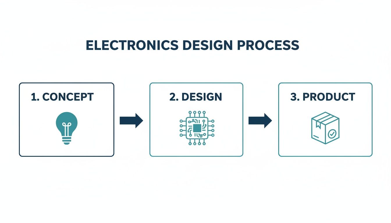
The Journey From a Great Idea to a Market-Ready Product
A working prototype is a critical milestone, but the path from a lab-bench success to a mass-produced product is where many ventures fail. This transition is fraught with risks: unforeseen manufacturing constraints, supply chain volatility, and compliance hurdles can derail your timeline and budget.
An experienced electronics design partner provides a structured roadmap to navigate this journey, systematically identifying and mitigating risks at each stage. The goal is not just to make the product work, but to ensure it can be built, tested, and trusted at scale. This requires baking critical disciplines like Design for Manufacturability (DFM) and Design for Test (DFT) into the process from the very beginning, not treating them as afterthoughts.
Discovery and Architecture: The Foundation for Success
Every successful program begins with a rigorous discovery phase. This is more than a feature checklist; it’s a systematic effort to map risks, define the system architecture, and establish unambiguous acceptance criteria. This foundational stage is non-negotiable for aligning engineering efforts with business outcomes.
Key deliverables from this phase should include:
- System Requirements Document (SRD): A formal document capturing all functional, performance, and compliance requirements.
- Architecture Decision Log (ADL): A record of key technical choices and their justifications, crucial for traceability and future design iterations.
- Initial Bill of Materials (BOM) Analysis: An early assessment of cost, lead times, and supply chain risks for critical components.
EVT, DVT, and PVT: The Gated Development Process
Product development is managed through a series of gated builds: Engineering Validation Test (EVT), Design Validation Test (DVT), and Production Validation Test (PVT). These are not merely phases; they are quality gates that a product must pass before proceeding, ensuring problems are caught early when they are least expensive to fix.
EVT (Engineering Validation Test): The primary goal is answering, “Does the fundamental design work?” This stage focuses on bringing up the first hardware, verifying core functionality (power, clocks, basic I/O), and identifying major architectural flaws. A small number of units are built, often requiring manual rework to debug.
Prototyping is inherently iterative. Overcoming Limitations in Prototyping often requires a strategic approach to debugging and validation.
Once the design is functionally proven at EVT, the focus shifts to DVT. Here, the question becomes, “Does the product meet all requirements in its intended environment?” DVT units are built using production-intent parts and processes to validate the design against the full SRD.
Finally, PVT validates the manufacturing process, not the product design. The goal is to prove that the product can be built at volume, using the final production line and fixtures, while meeting targets for quality, yield, and cycle time. You can learn more about this critical transition in our guide to PCB design for manufacturing.
This methodical approach is reshaping the industry. The electronics manufacturing services market is projected to grow from USD 647.18 billion in 2025 to USD 903.05 billion by 2031, with original design manufacturing (ODM) as the fastest-growing segment. This demonstrates a market shift toward partners who provide end-to-end design and manufacturing expertise.
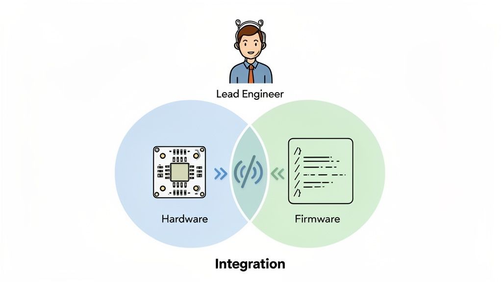
Integrating Hardware and Firmware Development
Treating hardware and firmware as separate, sequential tasks is a primary cause of integration failure, schedule delays, and product instability. The disciplines are deeply coupled; a hardware component choice directly impacts firmware complexity, and a firmware timing requirement can dictate hardware architecture. High-performing engineering teams place both disciplines under single-threaded technical leadership to ensure tight collaboration and rapid, informed iteration.
This integrated model means firmware considerations influence the design from the first schematic. For example, Design for Test (DFT) becomes a practical tool, not an academic exercise. Adding a few targeted test points to a PCB, a decision made during schematic capture, can radically simplify manufacturing test firmware, reducing fixture complexity and slashing production cycle times.
Critical Intersection Points for Hardware and Firmware
Successful product development hinges on managing the handoffs at key technical milestones. Failure to align at these points bakes in risk that often remains hidden until late in the development cycle, when fixes are most expensive.
- PCB Bring-Up: This is the first moment of truth. Does the board power on correctly? Can the firmware establish communication with critical peripherals? A collaborative team can diagnose power sequencing, clock stability, and boot chain issues in hours, not weeks.
- Sensor Integration: The analog front-end (AFE) hardware must be co-designed with the firmware’s signal processing algorithms. A mismatch results in noisy, unreliable data that cannot be fully corrected in software.
- Power Integrity: Firmware behavior is dynamic. Sudden changes in processor load can cause voltage transients that destabilize the system. Hardware must be designed to handle these software-driven events, ensuring the power delivery network (PDN) remains stable under all operating conditions.
The goal is to eliminate the “over the wall” mentality. When a firmware engineer can influence the schematic to add necessary debug hooks, and the hardware engineer understands the firmware’s real-time constraints, the entire program accelerates. This principle is core to how we execute at Sheridan Technologies.
Designing for Reliability and Maintainability
This synergy extends beyond initial product launch to long-term reliability. Robust firmware depends on hardware support. A reliable over-the-air (OTA) update mechanism with safe rollback capabilities requires hardware features like dual-bank flash memory, designed in from the start. Similarly, hardware watchdogs and brownout detectors are hardware/firmware contracts that provide essential fault tolerance.
By linking these technical decisions to business outcomes, an integrated approach delivers tangible value. A testable design lowers manufacturing costs. A reliable OTA update system reduces warranty claims and enables post-launch feature delivery. This holistic perspective is the hallmark of modern electronics design services.
For a deeper look at the software side of this equation, see our guide on embedded software development services. Integrating hardware and firmware is not just an engineering best practice; it is a strategic imperative for shipping complex products successfully.
How to Choose the Right Design Services Partner
Selecting an electronics design partner is a critical decision that can determine a product’s success or failure. The right partner acts as a force multiplier, accelerating your timeline while systematically de-risking the program from architecture to production. The wrong one can lead to missed deadlines, budget overruns, and a design that is difficult or impossible to manufacture.
The key is to look beyond marketing materials and evaluate a firm’s technical depth, process maturity, and manufacturing readiness. It’s not about finding the lowest bidder; it’s about identifying a team with a proven track record on high-stakes projects. Honing your process for choosing a service partner is a high-leverage activity for any technical leader.
This checklist provides a framework for vetting potential partners.
Partner Evaluation Checklist
Use these questions to drive substantive conversations that reveal a firm’s true capabilities and operational discipline.
| Evaluation Area | What to Look For | Key Questions to Ask |
|---|---|---|
| Technical Depth | A systems-level, physics-based understanding of trade-offs. Ability to anticipate integration issues and own the entire design. | “Walk me through a risk burn-down chart from a recent program.” “How do you approach power integrity analysis for a system with high transient loads?” “Describe a time a DFM constraint forced a significant change in the firmware architecture.” |
| Process Maturity | Disciplined documentation, rigorous verification strategy, and clear, gate-driven development milestones. Evidence of a repeatable process. | “What does your design review process look like, and who is involved at each gate?” “How do you manage requirements traceability through verification and validation?” “Can you share a redacted example of a final design transfer package?” |
| Manufacturing Readiness | A “design for manufacturing” (DFM) and “design for test” (DFT) mindset from day one. Deep experience with factory bring-up, fixture development, and yield optimization. | “At what stage are DFM/DFT analyses formally introduced?” “Describe your process for managing the EVT to DVT to PVT transitions.” “What is your experience developing a manufacturing test plan and collaborating with contract manufacturers?” |
These questions are designed to move beyond surface-level claims and assess how a team thinks, operates under pressure, and solves complex problems. A capable partner will welcome this level of scrutiny.
Evaluating Technical Depth
True technical depth is not a list of technologies on a website. It is the practical ability to reason about system-level trade-offs and anticipate second-order effects. A team with genuine depth makes architectural choices that prevent problems months down the line. Look for a structure that promotes single-threaded ownership, where one technical lead is accountable for the successful integration of hardware, firmware, and manufacturing. This model eliminates the siloed handoffs that are a common source of failure.
Assessing Process Maturity
A mature development process is the operational backbone that ensures consistent, high-quality outcomes. It is what separates teams that deliver successfully on occasion from those that can execute complex programs predictably, time after time. Evidence of maturity is found in rigorous documentation, formal verification strategies, and adherence to gate-driven milestones. This is non-negotiable in regulated industries like medical (ISO 13485) or aerospace (DO-178C), where the process artifacts are as critical as the product itself.
A partner’s process maturity is directly reflected in the questions they ask you. If they aren’t pushing back on requirements, asking tough questions about use cases, and challenging your assumptions, they aren’t doing their job as a strategic partner.
Gauging Manufacturing Readiness
Ultimately, a design is only successful if it can be built, tested, and shipped at scale with predictable yield and cost. The best partners design for manufacturability (DFM) and testability (DFT) from the initial concept. They understand from direct experience how a seemingly minor design choice can have major downstream impacts on factory operations. Probe their experience with the critical handoff from engineering to production, such as the DVT-to-PVT transition. Ask about their approach to developing manufacturing test plans and managing contract manufacturer (CM) relationships. This operational knowledge is what distinguishes a true product development partner from a prototyping service. For a deeper analysis, see our guide on engineering design services.
Avoiding Common Pitfalls in Product Development
Even brilliant product concepts can be derailed by predictable, preventable mistakes. We’ve seen it firsthand: an unmanaged Bill of Materials (BOM) creates a supply chain crisis, halting production over a single component. A poorly documented design is thrown “over the wall” to a contract manufacturer, resulting in months of costly rework. These are not minor technical issues; they are significant business risks that erode margins and cede market share to competitors. A true design partner serves as your first line of defense against these failure modes.
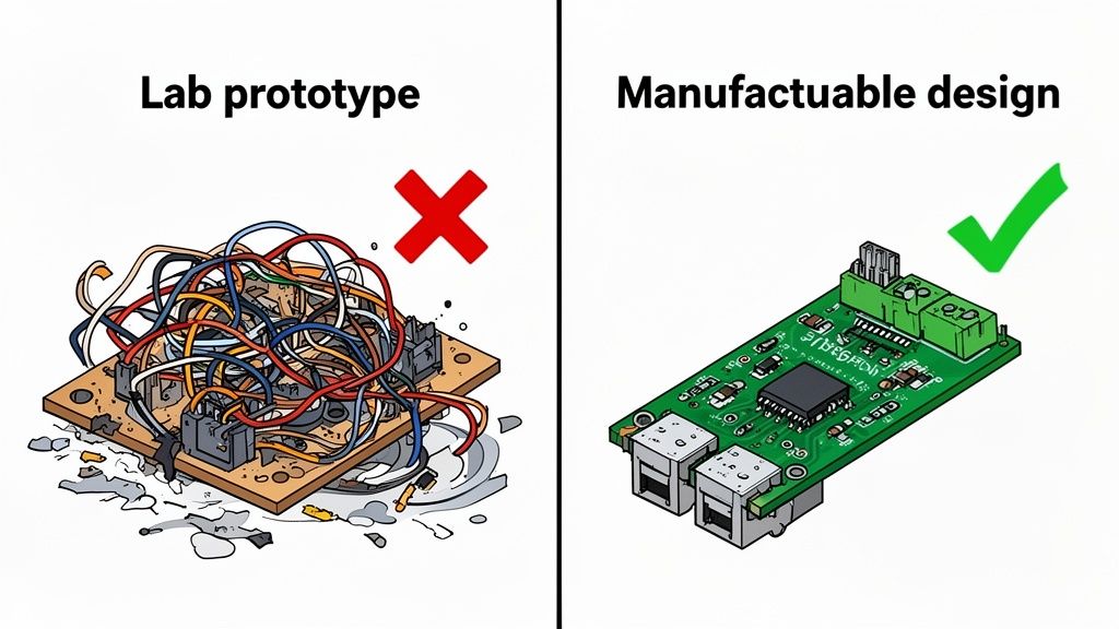
From “Lab Queen” to Production Reality
One of the most common traps in product development is the “lab queen” prototype—a single unit that performs perfectly on the bench but is held together by hand-selected components and manual tweaks. This type of prototype is often impossible to manufacture reliably or cost-effectively. The antidote is to integrate Design for Manufacturability (DFM) analysis throughout the entire development process, not as a final checklist item.
From the moment a component is placed on a schematic, an experienced partner is asking: “Does this part have multiple qualified sources? Can this be assembled efficiently by machine? Can we test this board in under 30 seconds on the production line?” These questions drive practical, production-oriented decisions early, preventing the “lab queen” from ever jeopardizing the launch.
Early Warning Signs and Mitigation Strategies
Identifying the early signals of a project heading off course is a critical skill for any engineering leader. Here are two common failure modes and proven strategies to mitigate them.
Failure Mode 1: The Brittle BOM. The Bill of Materials relies on single-source, long-lead-time, or near-end-of-life components.
- Early Warning Sign: Key components have lead times exceeding the prototype build schedule or lack qualified second sources.
- Mitigation Strategy: Implement a managed BOM process from day one. This involves continuously scrubbing the parts list for supply chain risk, designing in pre-qualified alternates, and engaging with suppliers early to secure allocation.
Failure Mode 2: The “Over-the-Wall” Handoff. The design team considers their job done after sending a data package to the contract manufacturer (CM).
- Early Warning Sign: The CM immediately returns with numerous basic questions about design intent, test procedures, or component placement that should have been explicit in the documentation.
- Mitigation Strategy: Involve the CM in DFM reviews early in the design cycle. Develop a comprehensive design transfer package that includes not only schematics and Gerber files but also detailed assembly instructions, test specifications, and programming procedures.
This disciplined, risk-reduction methodology is why the outsourced electronics design and manufacturing market is projected to grow from USD 635.49 billion in 2025 to USD 1.17 trillion by 2035. This growth reflects a strategic shift toward partners who can deliver production-ready systems and navigate today’s complex supply chains. You can explore the global electronic contract manufacturing market trends for more detail. An expert partner elevates the engagement from task execution to strategic risk management.
Frequently Asked Questions About Electronics Design Services
When engaging an external engineering partner, several key operational questions consistently arise. Addressing these points clearly upfront builds a foundation of trust and ensures smooth project execution. Here are the answers to the most common questions we hear from technical leaders.
What Is the Typical Cost Structure for an Engagement?
The pricing model for a project is typically determined by its level of definition. For projects with a well-defined scope and clear deliverables, a fixed-bid model is often appropriate, with payments tied to the achievement of major milestones (e.g., schematic completion, prototype delivery). For more open-ended research and development efforts where requirements are expected to evolve, a time-and-materials (T&M) model provides the necessary flexibility for iterative discovery and design.
How Is Intellectual Property Handled?
This is straightforward and non-negotiable: the client retains 100% ownership of all intellectual property (IP) created during the engagement. A reputable partner will codify this in the Master Services Agreement (MSA) or Statement of Work (SOW). All schematics, source code, design files, and documentation developed for the project are the exclusive property of the client.
What Level of Involvement Is Required From Our Team?
A successful partnership is collaborative. While our team executes the detailed design and verification work, your team’s role is crucial in providing the product vision, market context, and strategic direction. Your team’s involvement will be most intensive during several key phases:
- Initial Discovery and Requirements Definition: To ensure alignment on goals and constraints.
- Weekly or Bi-Weekly Reviews: To monitor progress, address technical roadblocks, and make key decisions.
- Formal Gate Reviews: To provide sign-off at critical milestones, such as design freeze before a prototype build.
How Long Does It Take to Get a Production-Ready Prototype?
Timelines vary based on product complexity, but a general estimate for a moderately complex IoT device is three to four months from project kickoff to a production-ready DVT (Design Validation Test) prototype. A more complex system, such as a regulated medical device, could take nine months or longer. Key drivers of the schedule include component lead times, firmware complexity, and the rigor of any required regulatory compliance testing (e.g., FCC, CE, IEC 60601). A credible partner will provide a detailed project plan that accounts for these variables.
What’s Next? Turning Your Idea Into a Market-Ready Product
A great idea is just the starting point. Successfully launching a complex electronic product means weaving together hardware, firmware, and manufacturing readiness right from the get-go.
As we’ve seen, designing for manufacturability and testability isn’t a final step you tack on at the end—it’s the core strategy. It’s how you cut down program risk, get a handle on costs, and actually speed up your time-to-market. The most critical decision you’ll make is choosing a partner who lives and breathes this discipline.
Time to put these insights into action. Take a hard look at your current project’s documentation. Is it truly ready for manufacturing? Go through your verification plan—how solid is your test coverage? High-performing teams are constantly de-risking their programs by obsessing over these crucial handoffs.
When you’re ready to move beyond theory and start solving real-world engineering challenges, the right conversation can change everything.
At Sheridan Technologies, we specialize in spotting and neutralizing program risks before they can derail your launch. Skip the guesswork and move straight to solving problems with a Manufacturing Readiness Assessment.