
Ignoring your PCB test strategy is a direct path to field failures, costly recalls, and catastrophic schedule delays. A failed board can halt an entire production line, erode margins, and damage your company’s reputation. For engineering leaders and program managers, the stakes are high. The problem is that many teams treat testing as a final, reactive step, inviting risk and unpredictability into their programs. Effective PCB testing isn't about picking one method; it's about implementing a phased verification strategy that de-risks the product at every stage, from first prototype to high-volume manufacturing.
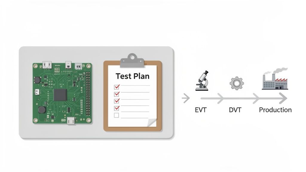
This guide is for the VPs of Engineering, Program Managers, and Lead Engineers responsible for shipping reliable hardware on schedule. It’s for those operating under tight constraints where time-to-market, budget, and quality are non-negotiable. This is not a guide for hobbyist projects where failures are inconsequential. We'll frame PCB testing as a strategic, risk-reduction activity, showing how to align test methods with your development gates (EVT/DVT/PVT) to achieve predictable outcomes.
By following this framework, you will learn to:
- Structure a phased test plan that catches critical defects early, when they are cheapest to fix.
- Select the right test methods (ICT, Flying Probe, JTAG) based on volume, complexity, and program risk.
- Integrate Design for Test (DFT) principles early to reduce manufacturing friction and improve yield.
Foundational Testing: De-risking Early Prototypes (EVT)
There’s nothing like the first power-up of a new prototype. It's the moment of truth in your Engineering Validation Test (EVT) phase, a checkpoint that answers one huge question: is this board even alive? It’s tempting to just plug it in, but that’s a rookie mistake that can end with fried components and days of needless debugging. Before a single electron flows, the real work begins with meticulous, non-powered checks. This is your first and best line of defense against common assembly defects that cause catastrophic failures. Skipping this step is like building a house on a shaky foundation—the problems will only get worse and more expensive.
Pre-Power-Up Inspection Checklist
Your first move should be to get that board under a high-magnification scope for a thorough, methodical inspection. You can catch a surprising number of assembly errors with a good set of eyes before they cause damage.
- Solder Joint Quality: Hunt for solder bridges between pins, especially on fine-pitch components like MCUs and BGAs. Look for cold or incomplete joints, which are notorious for creating frustrating, intermittent open circuits.
- Component Placement & Polarity: Do a quick inventory. Are all components present? Are they oriented correctly? Check the polarity marks on diodes and electrolytic capacitors. Have any components tombstoned during reflow?
- Debris and Contamination: Look for stray solder balls, excessive flux residue, or other contaminants that could create an unexpected short circuit. A quick blast of compressed air is your best friend here.
- Bare-Board Shorts: The best practice is to test the bare PCB before assembly, but you still need to check populated boards. Grab a multimeter in continuity mode and probe the primary power rails—like VCC and GND. If that meter beeps, you have a dead short. Stop everything and fix it.
Failure Mode: A short between a main power rail and ground is one of the most common—and destructive—faults on a new board. Finding it with a multimeter takes seconds. Finding it with a power supply often results in a puff of magic smoke, a damaged prototype, and a schedule slip of days or weeks.
Systematic Power-Up and Verification
Once the board is visually clean and passes the short-circuit test, you're ready for a controlled power-up. The goal isn't full functional validation. It’s to establish basic power integrity and confirm signs of life.
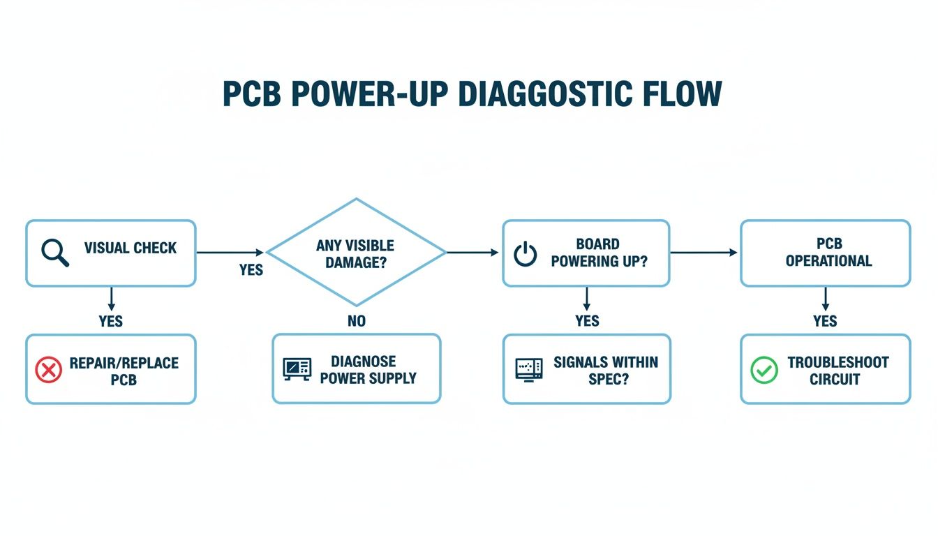
Use a current-limited bench power supply. Set the voltage to its nominal level but crank the current limit down to 50-100mA to start. This is your safety net. If an undetected short exists, the supply will trip before it melts anything. If the current draw is stable, you can slowly dial up the limit.
With stable power applied, methodically probe each voltage rail with an oscilloscope. You're looking for two things:
- Correct Voltage Level: Is your 3.3V rail actually at 3.3V?
- Signal Quality: Is the rail clean, or is it full of noise and ripple? Poor power integrity is a recipe for baffling stability issues later.
After confirming all power rails are stable, check for the board's "heartbeat." Scope the main clock and crystal oscillator outputs. Finally, establish basic communication. This is often done with a UART connection or, more powerfully, by connecting a JTAG/SWD debugger. If you can connect to the processor, halt it, and read registers, you've successfully brought your board to life. For a deeper look, explore advanced methods for debugging with JTAG to quickly diagnose complex issues.
Scaling Verification: Automated Testing for DVT and Production
Manual bench tests are essential for bringing up first prototypes, but they don't scale. As you move into the Design Validation Test (DVT) phase and prepare for production, manual testing cannot deliver the speed, coverage, or repeatability required. This is where you must scale your verification strategy with automation. It’s a crucial step in orchestrating a smooth new product introduction and involves making strategic trade-offs between speed, cost, and fault coverage. Your decision will likely boil down to a few key automated test methods.
In-Circuit Testing (ICT): The High-Volume Powerhouse
Think of In-Circuit Testing as the heavy artillery of manufacturing test. It uses a custom "bed-of-nails" fixture with pogo pins that press against hundreds of designated test points on the board simultaneously. This brute-force approach allows an ICT station to perform a comprehensive component-level check in seconds, looking for:
- Shorts and opens
- Correct values for passive components (resistors, capacitors)
- Presence and orientation of diodes and transistors
- Basic checks on integrated circuits
The catch? The non-recurring engineering (NRE) cost to design and build the custom fixture is significant. If your PCB layout changes, you're buying a new fixture. This makes ICT ideal for stable, high-volume products where the initial cost is amortized across thousands of units, driving the per-board test cost toward zero.
Flying Probe Testing: The Flexible Prototyping Ally
For early-stage products and smaller runs, the flying probe tester is your best friend. This method uses two or more robotic probes that "fly" across the board to test component pads and vias directly, eliminating the need for a costly fixture.
The primary advantage is flexibility. When the design changes, you just update the test program—no new hardware, no massive NRE bill. This is invaluable during DVT when you might be spinning a new board revision every few weeks.
The trade-off is speed. A flying probe test can take several minutes per board, a lifetime compared to the seconds an ICT requires. It's not economical for mass production, but it’s the go-to choice for prototyping and low-volume manufacturing where agility is paramount.
Comparison of Automated PCB Test Methods
Choosing between these methods is a strategic decision based on volume, design maturity, and budget. The right strategy for a 50-unit prototype run is completely different from one for a 50,000-unit production ramp.
| Test Method | Best For | Speed | Upfront Cost (NRE) | Fault Coverage | Flexibility to Changes |
|---|---|---|---|---|---|
| In-Circuit Test (ICT) | High-volume, stable designs | Very Fast (seconds/board) | Very High | Excellent (component-level) | Very Low |
| Flying Probe | Prototypes, low/mid-volume | Slow (minutes/board) | Low to None | Good | Very High |
| Boundary Scan (JTAG) | Dense boards with BGAs | Moderate | Low (if ICs are compliant) | Good (digital interconnects) | High (software-based) |
Ultimately, this isn't an either/or choice. High-performing teams often use a hybrid approach: flying probe for early runs, JTAG to cover BGAs, and a full ICT once the design is locked for mass production.
Boundary Scan (JTAG): Testing the Untestable
What happens when your board is so dense with BGAs that you can't physically reach the test points you need? This is an increasingly common problem.
The solution is Boundary Scan, often implemented via a JTAG interface. This technique builds testability into the silicon of compliant ICs. It creates a digital chain linking the I/O pins of major chips, letting you send signals to verify every connection between them—all without a single physical probe. This makes JTAG essential for confirming the thousands of hidden solder joints under BGAs are free of shorts or opens. As boards become more complex and physical test access shrinks, Boundary Scan shifts from a "nice-to-have" to a fundamental necessity.
System-Level and Environmental Validation (PVT)
A board can pass every benchtop and automated test yet fail spectacularly in the real world. This is the crucial gap that system-level and environmental validation are designed to close. Here, we move beyond isolated checks to answer the one question that truly matters: will this product survive and perform as intended in the hands of the end-user? For experienced teams, this isn't a final checkbox; it's a critical risk-reduction step that proves the entire system—hardware, firmware, and mechanics—works in harmony under realistic, and often stressful, conditions.
Simulating Reality with Functional Test Fixtures
Before subjecting a board to extreme heat or vibration, you must verify it functions as a complete system. This is where a Functional Circuit Test (FCT) comes in. An FCT fixture is a custom-built environment engineered to simulate the board's real-world inputs and monitor its outputs, exercising the product as a user would.
- Simulating Inputs: The fixture might include physical buttons or emulate digital signals that mimic sensor data or communication from other subsystems.
- Loading All Outputs: Instead of just checking for a voltage, the fixture connects to the actual motors, displays, and communication ports to ensure they behave as expected under a real electrical load.
- Running End-to-End Scenarios: The test sequence executes firmware-driven routines, verifying that a specific input produces the correct output within the required time.
A well-designed FCT is the closest you can get to putting the final product in a customer's hands without shipping it. It moves the question from "Is this component soldered correctly?" to "Does this feature actually work?"—a critical distinction for validating product requirements before the costly Production Validation Test (PVT) stage.
Uncovering Latent Defects with Environmental Stress
Once functional performance is confirmed, the next job is ensuring reliability over time and across operating conditions. Environmental testing is designed to accelerate failure modes and expose latent defects that would never show up on a lab bench. For products in demanding fields like medical, industrial, or aerospace, these tests are non-negotiable.
- Thermal Cycling: The device is subjected to rapid temperature swings between its maximum and minimum operating specifications. This process stresses solder joints and mechanical components, quickly revealing weaknesses caused by mismatched coefficients of thermal expansion (CTE).
- Vibration and Shock: The board, often mounted in its final enclosure, is put on a shake table to simulate everything from transportation rattling to operational vibrations. Shock tests simulate drops or impacts to ensure components don't dislodge.
Accelerating Early Failures with Burn-In Testing
The final gatekeeper, especially for high-reliability products, is burn-in testing. This process involves running the device continuously—often at an elevated temperature and under full electrical load—for anywhere from 12 to 168 hours. The logic is rooted in the "bathtub curve" of electronics reliability, which shows a high rate of early-life ("infant mortality") failures caused by subtle manufacturing defects. Burn-in testing is designed to aggressively push these weaker units past their breaking point before they leave the factory, preventing costly field returns and protecting your brand's reputation.
The increasing complexity of modern electronics has fueled significant growth in the PCB testing market. This trend, driven by the need for more advanced validation techniques like these, is explored in market analyses of PCB testing market growth drivers, underscoring that the demand for thorough system-level and environmental verification is only intensifying.
Designing for Testability (DFT): A Strategic Imperative
The most expensive problems are always the ones you can't find. Testability isn't something you bolt on at the end; it’s a core design discipline you bake in from the first schematic. This proactive approach is called Design for Testability (DFT), and it is the single most effective way to cut costs, reduce diagnostic time, and slash program risk. DFT reframes the development process: instead of asking, "How can we test this finished board?", it forces the question, "How will we make this board easy to test?" from the start. The impact on the bottom line is immediate—less complex fixtures, shorter test cycles, simpler failure analysis, and higher production yields.
The Core Pillars of a Strong DFT Strategy
Making hardware testable comes down to a few fundamental practices. For any complex product, these are critical for hitting quality and schedule targets.
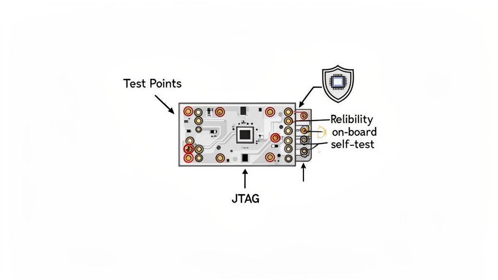
- Strategic Test Point Placement: This is DFT 101. Deliberately add accessible pads or vias on critical nets so you can get a probe on them during flying probe, ICT, or bench debugging.
- JTAG/Boundary Scan Implementation: For designs with complex ICs like FPGAs or BGAs, a fully implemented JTAG chain is non-negotiable. It provides digital access to check thousands of connections that are physically impossible to probe.
- Built-in Self-Test (BIST): This is where you get clever with firmware. Design routines that run power-on self-tests (POST), check memory integrity, or verify peripheral functions, empowering the board to test itself without external equipment.
Business Impact: A few hours spent adding test points and planning a JTAG chain during layout can save hundreds of engineering hours debugging mysterious failures during DVT or dealing with field returns after launch. DFT is a massive force multiplier for quality and a key tenet of how high-performing teams practice PCB design for manufacturing at Sheridan.
Real-World Scenario: The Industrial Controller Redesign
A team I worked with was developing an industrial robotic arm controller. The first prototype was a nightmare to diagnose—no dedicated test points, and the JTAG chain was an afterthought. Any intermittent failure became a heroic, time-sucking debugging effort that put the schedule at risk.
For the next revision, we mandated a DFT-first approach. We added test points for every power rail and critical signal. We implemented a complete boundary scan chain connecting all major ICs. And we required the firmware team to create a comprehensive self-test routine.
The results were stunning. The new boards could be put through a full, automated test suite in minutes. Using JTAG, we found a subtle assembly defect causing intermittent bus errors in less than an hour—a fix that would have taken days before. That early investment in DFT directly prevented a late-stage redesign and kept the production schedule on track.
At the end of the day, quality testing is about confidence in your measurements. This principle applies everywhere precision matters, from the factory floor to the research lab. Whether it's calibrating a million-dollar test fixture or mastering calibration for precise lab results, the goal is the same: trustworthy data. DFT is how you build that trust into the DNA of your product.
What to do Monday Morning: Your Next Steps
Even with a solid plan, engineering leaders often circle back to a few key questions. This section provides clear, operational answers to help you make strategic decisions.
How Much Testing Is Enough?
The honest answer is: it depends on your product's risk profile. The goal isn't 100% coverage, which is often economically impossible. The goal is to match your test investment to the consequences of a failure. A good way to frame this is to bucket potential failures by impact:
- Safety-Critical Failures: Any failure that could lead to harm or regulatory action (e.g., in medical or aerospace). These demand the most rigorous, redundant testing. No compromises.
- Mission-Critical Failures: Failures that brick the product and will almost certainly result in a field return. These justify significant investment in automated functional and burn-in testing.
- Minor Annoyances: Issues that degrade user experience but don’t stop the product from working. Coverage here can be lighter, as these are often caught during system-level tests.
Mapping your test plan to these risk categories shifts the conversation from a vague goal of "thorough testing" to a quantifiable strategy of risk mitigation. This is how high-performing teams justify their test budget.
Can We Skip Fixtures And Just Use Flying Probe?
Relying exclusively on flying probe testing as you scale is a classic trap that can cripple your manufacturing throughput.
The core trade-off is simple: flexibility versus speed. A flying probe test might take 5-10 minutes per board, while a full In-Circuit Test (ICT) with a bed-of-nails fixture can test that same board in under 60 seconds.
For your first few prototype runs (EVT), the flexibility of the flying probe is a clear winner. But once your design stabilizes and you're facing production volumes in the thousands, the math flips. The high NRE for an ICT fixture is quickly absorbed by the massive drop in per-unit test time. The best strategy is often a phased one: start with flying probe, then invest in ICT for mass production.
When Should We Bring In Our Contract Manufacturer?
The answer is simple: much earlier than you think. Too many teams treat their Contract Manufacturer (CM) like a simple vendor, handing over a finalized design and a test plan as a done deal. This is a massive missed opportunity.
Your CM possesses invaluable knowledge on Design for Manufacturability (DFM) and Design for Testability (DFT). Bringing them in during schematic capture and layout provides critical insights that make your board dramatically easier and cheaper to build and test. They can advise on:
- Test point placement that works best with their specific equipment.
- Panelization strategies optimized for their automated test flow.
- Component selections that are more readily available, reliable, and testable.
Engaging your CM early transforms them from a supplier into a strategic partner. This collaborative approach is a hallmark of teams that successfully navigate the path from prototype to production with fewer surprises. And for boards that don't pass testing or reach their end-of-life, understanding the proper methods for their disposal of printed circuit boards is also a key consideration in a complete lifecycle plan.
At Sheridan Technologies, we believe that a proactive, integrated test strategy is the foundation of every successful product launch. We design for testability from day one, reducing program risk and ensuring a smooth transition from prototype to production. If you're facing challenges with your current verification plan or need to de-risk an upcoming product, a manufacturing readiness assessment can provide the clarity you need.