
Choosing the hardware for an embedded system is one of the most consequential decisions a product team will make. Getting it right provides a stable foundation for development and manufacturing. Getting it wrong can trigger late-stage redesigns, budget overruns, and catastrophic schedule delays that put a program’s success in jeopardy. When the hardware fails to meet operational requirements, you’re not just fixing a bug—you’re often forced back to the drawing board, losing critical time-to-market.
This guide is for the engineering leader, program manager, or lead engineer responsible for making architectural hardware decisions that align with real-world business outcomes. It provides a decision-making framework for moving a product from a functional prototype to a reliable device that can be manufactured at scale and trusted in the field. This guide will help you navigate the essential tradeoffs and decisions by covering:
- Core Processor Selection: Making the right call between an MCU, MPU, and SoC based on system requirements and business constraints.
- Design for Manufacturing and Test (DFM/DFT): Building in testability and production readiness from the very first schematic.
- Prototype-to-Production Readiness: De-risking the path from a working model to a market-ready, scalable product.
Choosing Your Core Processor: MCU, MPU, or SoC
At the heart of any embedded system lies its processor—the brain that sets the ceiling for what your device can achieve. This choice between a Microcontroller Unit (MCU), a Microprocessor Unit (MPU), or a System-on-Chip (SoC) is a critical architectural decision. It fundamentally defines your product's performance, power budget, bill of materials (BOM) cost, and the complexity of your firmware development.
Selecting an underpowered processor can lead to missed performance targets and frantic, late-stage redesigns. Conversely, choosing an overpowered and expensive chip risks bloating the BOM so much that the product becomes commercially unviable. The objective is to match the processor's capabilities to your immediate technical needs and the product's long-term business goals, striking a delicate balance between technical specifications and project constraints.
The Core Tradeoffs: MCU vs. MPU
The distinction between an MCU and an MPU is a foundational concept in embedded engineering.
An MCU is a self-contained specialist. It integrates a CPU, memory (RAM and Flash), and peripherals like timers, ADCs, and communication interfaces onto a single chip. This all-in-one design is ideal for specific, deterministic tasks where real-time control is paramount. You'll typically find MCUs running bare-metal code or a Real-Time Operating System (RTOS) to guarantee predictable responses to events.
An MPU, in contrast, is a powerful generalist. It features a much more capable CPU but relies on external components for RAM, storage, and often many peripherals. This modularity allows it to run a full-featured operating system, like embedded Linux, enabling complex applications, rich graphical user interfaces (GUIs), and sophisticated networking.
Sheridan Technologies' Take: We often see teams gravitate to an MPU for the flexibility of a full operating system. But for any hard real-time system—such as a motor controller in a robotic arm or a safety-critical medical sensor—an MCU’s deterministic behavior is a requirement, not a preference. The predictable timing of an RTOS-driven MCU frequently trumps the raw, general-purpose power of an MPU in these scenarios.
The flowchart below shows how a solid hardware selection process weighs these factors to drive a project toward success.
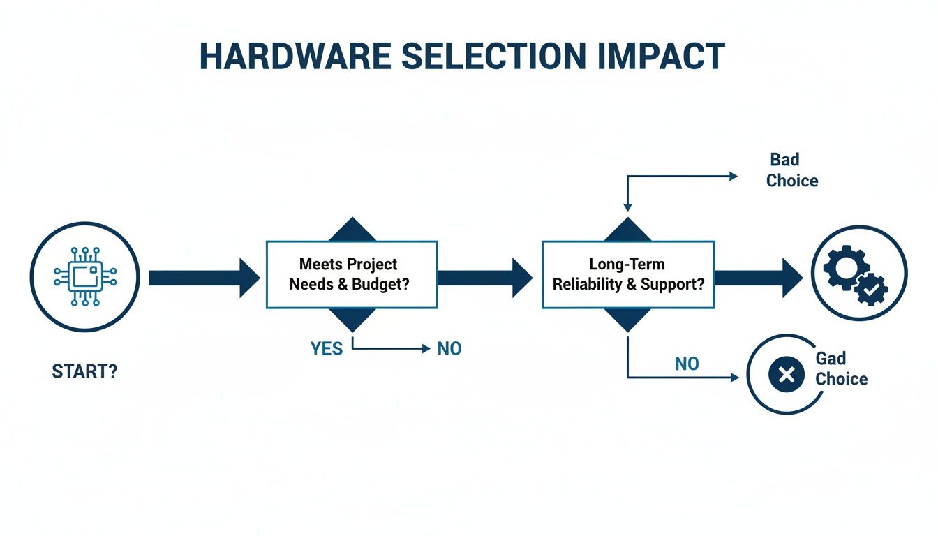
As the diagram illustrates, a "good choice" comes from systematically evaluating project needs, budget, and reliability from the very beginning. A "bad choice" almost always stems from skipping these crucial early assessments.
Enter the SoC: The Path to Integration
A System-on-Chip (SoC) takes integration a step further, squeezing an entire system onto a single piece of silicon. A modern SoC might contain one or more MPU cores, a dedicated MCU core for real-time tasks, a GPU for graphics, hardware accelerators for AI or video encoding, and a full suite of peripherals and wireless radios.
SoCs power modern consumer electronics, from smartphones to smart home hubs. Their main advantage is consolidation, delivering key benefits:
- Reduced Size: A smaller PCB footprint is critical for compact devices.
- Lower BOM Cost: One chip can replace dozens of discrete components.
- Improved Power Efficiency: Tightly integrated components allow for more granular power management.
However, this high integration introduces challenges. Developing firmware for a complex SoC can be a much heavier lift, and you are locked into the vendor's specific set of peripherals and power management schemes. For a deeper dive, our guide on understanding the role of a System-on-Chip breaks down these components in more detail.
The table below offers a practical decision matrix to help engineering leaders navigate these choices based on common project requirements.
MCU vs MPU vs SoC Decision Matrix for Embedded Systems
| Criterion | Microcontroller (MCU) | Microprocessor (MPU) | System-on-Chip (SoC) |
|---|---|---|---|
| Primary Use Case | Real-time control, specific tasks (e.g., motor control, sensor reading) | General-purpose computing, complex applications (e.g., GUIs, networking) | Highly integrated systems, consumer electronics (e.g., smartphones, smart TVs) |
| Operating System | Bare-metal, Real-Time Operating System (RTOS) | Full OS (Linux, Windows Embedded, Android) | Full OS, often with a secondary RTOS on a dedicated core |
| Performance | Lower, optimized for deterministic control | Higher, suitable for complex processing | Highest, often with multiple specialized cores (CPU, GPU, DSP, NPU) |
| Power Consumption | Very Low (µA to mA range) | Higher (mA to A range) | Optimized for efficiency but can be high under full load |
| BOM Cost | Low (Single chip solution) | Higher (Requires external RAM, Flash, peripherals) | Varies; can be lower than MPU + discrete parts, but high for advanced SoCs |
| PCB Footprint | Small | Large | Small to Medium (High integration reduces board space) |
| Development Complexity | Lower (Simpler architecture, fewer external dependencies) | Higher (OS-level development, driver integration, complex board design) | Highest (Complex firmware, vendor-specific tools, multi-core debugging) |
| Time-to-Market | Faster (for simple, well-defined tasks) | Slower (due to hardware and software complexity) | Can be fast with a good Board Support Package (BSP), but complex otherwise |
| Best For | IoT endpoints, industrial sensors, simple appliances, automotive controllers | HMI panels, network gateways, advanced medical devices | Smartphones, tablets, advanced robotics, AI-enabled edge devices |
Choosing the right processor is less about finding the "best" chip and more about finding the right chip for your specific application, budget, and timeline. Each path comes with its own engineering trade-offs. The growth in this market is undeniable; you can dig into more data on the embedded systems market here or explore more on the embedded systems market growth in our analysis.
Designing for Manufacturing and Test (DFM & DFT)
A brilliant prototype that works perfectly on your bench is a great milestone, but it’s dangerously far from a successful product. The critical gap between a single functional unit and a thousand reliable ones is bridged by two practices that must be baked in from the start: Design for Manufacturability (DFM) and Design for Testability (DFT).
These are not late-stage tweaks. They are core principles that must shape your hardware design from the very first schematic. Failing to think about production realities early on is a classic, costly mistake that causes schedule slips, budget overruns, and catastrophic yield issues at the factory. When a contract manufacturer (CM) can't efficiently build or test your design, every unit costs more in time and labor. Worse, untestable boards can hide defects that only show up in a customer's hands, leading to expensive recalls and a damaged reputation.
Operating Scenario: Industrial Automation Under Pressure
Picture this: an industrial automation company is ready to move their new controller from the Engineering Validation Test (EVT) stage to Design Validation Test (DVT). The pressure is on to freeze the design and hit a tight launch schedule. The stakes for reliability are sky-high—these controllers will run in harsh factory environments where a minute of downtime costs thousands of dollars. The EVT prototype works, but the PCB layout is dense. Critical signals are buried in inner layers with no accessible test points, and the team punted on defining a test fixture strategy, figuring they could "work it out later." This is a recipe for disaster. Pushing this design forward means they're building a product that’s expensive to make and nearly impossible to validate at scale.
Key DFT and DFM Strategies for Production Readiness
To sidestep that kind of train wreck, engineering leaders must treat DFT and DFM as non-negotiable requirements. This means embedding specific, practical features into the hardware long before it ever sees a production line.
Here are the essentials:
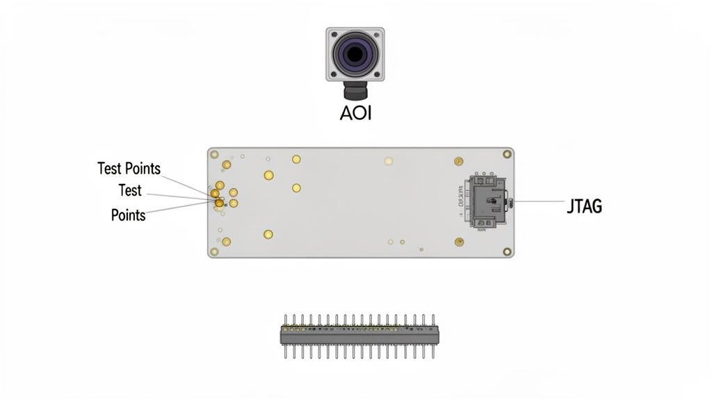
- Accessible Test Points: Every critical signal—power rails, clocks, resets, and key communication lines like I2C and SPI—needs a physical test point. These are your windows into the board's health during bring-up, debugging, and automated testing. Without them, you're flying blind.
- Robust Programming Interfaces: Design a reliable, easily accessible programming header (like SWD or JTAG) that can survive thousands of mating cycles on a production line. A flimsy connector or bad placement can bring manufacturing to a halt.
- Boundary Scan (JTAG): For complex chips like FPGAs and large MPUs in BGA packages, a JTAG chain is essential. It lets you automatically test the solder connections between chips without physical probes, catching otherwise invisible defects.
At Sheridan Technologies, we see this as fundamental. If you can't program a device and verify its core functionality in under 30 seconds on the line, your design isn't ready for manufacturing. Early DFT planning is one of the highest-leverage activities for reducing total product cost and program risk.
Designing for Automated Inspection and Assembly
Beyond testability, your layout must be optimized for the machines that will build your board. Component placement, trace routing, and panelization directly impact manufacturing yield and cost. Our guide on PCB design for manufacturing dives deeper into these details.
Here are a few DFM best practices to live by:
- Component Placement for AOI: Automated Optical Inspection (AOI) systems scan every board for placement errors. If you place components too close together or cover their markings, you break the automation and force expensive, slow manual review.
- Fiducials and Tooling Holes: Add fiducial markers to your PCB to give pick-and-place machines accurate reference points. Include tooling holes that align with your CM’s assembly jigs and test fixtures. Don't make them guess.
- Panelization Strategy: Work directly with your CM to define a panel layout that maximizes their machine efficiency and minimizes material waste. A bad panel design can lead to boards getting stressed or damaged during depanelization.
By embedding these DFM and DFT principles into your hardware process, you turn manufacturing from a massive risk into a predictable, scalable operation. This foresight is what separates the teams that ship successful products from those stuck in an endless loop of costly board revisions.
Power Management and Wireless Connectivity
Once you move past the processing core, two things truly make or break modern embedded hardware: how it sips power and how it talks to the rest of the world. These aren't separate engineering problems; they're deeply tangled together. Getting power management right is a dealbreaker for anything running on a battery, and without solid connectivity, your IoT product is just a fancy paperweight.
This section covers the system-level strategy for both, looking at the architectural choices that create a device that’s both power-frugal and a robust communicator, ready for the real world and the certification lab.
Designing an Efficient Power Delivery Network
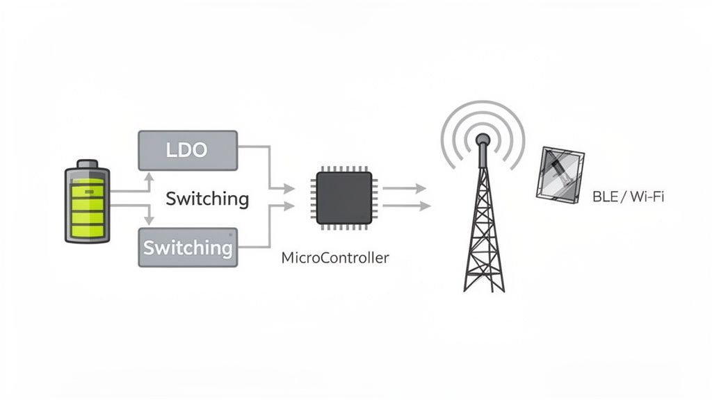
A core part of hardware for embedded systems is delivering clean, reliable power where it needs to go. A well-designed system starts with exploring the right power supply solutions for the job. The web of regulators, filters, and copper traces that gets power from the source to the chips is called the power delivery network (PDN). Get this wrong, and you’re in for a world of pain with instability, noise-induced crashes, and batteries that die prematurely.
Your two main tools for regulating voltage are Low-Dropout Regulators (LDOs) and switching regulators (DC-DC converters).
LDOs are the simple choice. They're straightforward, produce very little electrical noise, and are perfect for powering sensitive analog parts or providing a final, clean voltage to a specific component. The catch? They’re inefficient if your input voltage is much higher than your output, as they burn off the extra energy as heat.
Switching Regulators are the efficiency champs, often hitting >90% efficiency. This makes them a must-have for battery-powered devices. The trade-off is the switching noise they generate, which can wreak havoc on sensitive analog or RF circuits if you don't nail the filtering and layout.
A smart strategy is to use both: a high-efficiency switching regulator does the heavy lifting, and then small LDOs create pristine, localized power rails for noise-sensitive components like sensors or the radio.
Operating Scenario: An Ultra-Low-Power Agricultural Sensor
Let's make this real. Imagine you're building a remote sensor for a smart farm. The demands are brutal: it needs to run reliably for five years on a single coin cell and send its data over BLE just twice a day. This kind of challenge forces you to be absolutely ruthless about power consumption.
Here, the power budget isn't measured in milliamps; it's measured in microamps (µA). The device will spend nearly its entire life in a deep sleep state, waking for only a few seconds to take a measurement and transmit. Every single component choice is make-or-break. The MCU needs a deep sleep mode that draws less than 1 µA, and the BLE module has to have an exceptionally low current draw during its brief transmit and receive cycles.
Sheridan Technologies' Take: In these ultra-low-power designs, the quiescent current—the tiny bit of power a regulator uses just by being turned on—can actually become the biggest battery drain. Choosing a regulator with a quiescent current measured in nanoamps is just as vital as its conversion efficiency. A "highly efficient" switcher with a high quiescent current will absolutely kill a battery faster than a less efficient one in a device that spends 99.9% of its time asleep.
Integrating Wireless Connectivity and Managing EMI
Adding a radio like Wi-Fi or Bluetooth Low Energy (BLE) introduces another layer of complexity. The RF section is incredibly sensitive to noise, and its performance lives or dies by the antenna and its placement.
When you're integrating wireless, here's what you need to obsess over:
Antenna Selection and Placement: A PCB trace antenna is cheap but demands careful design and is easily detuned by nearby components. A ceramic chip antenna offers better, more predictable performance in a tiny package at a higher cost. The golden rule is to keep any antenna far away from metal cases, ground planes, and high-speed digital lines.
Impedance Matching: The path from the radio chip to the antenna is a transmission line that must be impedance-matched (usually to 50 ohms) to get maximum power out. Any mismatch causes signals to reflect backward, killing your range and performance.
EMI/EMC Management: Your device has to play nice with others. It can't just tolerate external interference (EMC); it also can't spew out so much noise that it interferes with other electronics (EMI). Passing EMI/EMC certification isn't optional for commercial products. Proper grounding, shielding, and filtering are your best friends here. As you map out your wireless plan, our guide on implementing Wi-Fi for IoT devices can offer some deeper insights.
For our agricultural sensor, the team would almost certainly opt for a pre-certified BLE module with an integrated antenna to sidestep the nightmare of custom RF design. They'd place it right at the edge of the PCB, as far as possible from the battery and the noisy switching regulator, to maximize its range and ensure it can reliably phone home from the middle of a field.
Integrating Sensors and Analog Front-End Design
For an embedded system to be useful, it has to accurately perceive the world around it. This is where the magic—and a lot of the challenge—happens. It involves taking real-world phenomena like pressure, light, or temperature and turning them into clean digital signals the processor can understand.
This crucial intersection of the physical and digital worlds is handled by the Analog Front-End (AFE). Get this part wrong, and nothing else matters. No amount of clever code can save a system that's fed garbage data from the start. The AFE’s job is to take a raw, often faint and noisy, analog signal and prepare it for conversion: amplifying it, filtering out interference, and ensuring what’s left is a stable, true representation of reality.
Operating Scenario: A Robotics Team's Grasping Challenge
Picture a robotics team building a new gripper to handle a delicate object, like an egg, without crushing it. This requires incredibly precise force feedback. They decide to use a strain gauge, a simple sensor whose electrical resistance changes slightly when it's stretched or compressed.
But here’s the problem: that change in resistance creates a signal that is minuscule—in the microvolt range. It’s easily lost in the sea of electrical noise generated by the robot's own powerful motors.
The team's success hinges on a few key decisions:
- Sensor Selection: Is the strain gauge sensitive enough? Does it physically fit on the robotic finger?
- AFE Design: How do they build an amplifier circuit that can reliably boost that tiny, fragile signal?
- Signal Integrity: How must they design the circuit board to shield the sensitive analog path from the noisy power lines feeding the motors? One stray trace could corrupt everything.
Translating the Physical World to Digital Data
At its core, the AFE is all about amplification and filtering. For a sensor like our strain gauge, the raw signal is often buried in the microvolt (µV) range. The perfect tool for this is an instrumentation amplifier, a specialized circuit designed to amplify these tiny differences while aggressively rejecting any noise that appears on both input lines.
Once amplified, the signal still isn't clean. High-frequency noise from digital clocks or switching power supplies can easily contaminate the measurement. A well-designed low-pass filter is non-negotiable; it acts as a gatekeeper, stripping away this electrical junk before the signal moves on.
A classic pitfall we see at Sheridan Technologies is improper grounding on a PCB. When analog and digital grounds are carelessly mixed, noise from the digital side bleeds directly into your sensitive analog signals. Suddenly, your measurements are useless. A star ground configuration or a carefully partitioned ground plane isn't just a best practice—it's often a hard requirement.
Choosing the Right Analog-to-Digital Converter
The final piece of the puzzle is the Analog-to-Digital Converter (ADC), which translates the clean, conditioned analog voltage into a number the microcontroller can use. Picking the right ADC comes down to two main parameters:
- Resolution (bits): This defines the precision of the measurement. A 12-bit ADC splits the voltage range into 4,096 discrete steps, while a 16-bit ADC offers a much finer 65,536 steps. For the robotics team, higher resolution means the robot can detect much smaller changes in grasping force.
- Sampling Rate (samples per second): This is how often the ADC takes a measurement. For a slow-changing signal like ambient temperature, a few samples per second is plenty. But for capturing a rapid force change, you need a much higher rate to avoid missing critical moments.
For their gripper, the team would likely choose a 16-bit ADC with a moderate sampling rate. This gives them the precision needed for fine motor control without overwhelming the processor with unnecessary data. Furthermore, building in robust connectivity allows for real-time monitoring and diagnostics, a concept widely used in industrial settings with IoT sensors for predictive maintenance. By thoughtfully designing the AFE and selecting the right ADC, the robotics team ensures their MCU gets trustworthy data—the foundation for the delicate control they set out to achieve.
Navigating from Prototype to Production
Getting that first prototype to work is a huge win, but it’s just the starting line. The road from a single, functional board on your bench to a scalable, reliable product ready for the market is where most hardware ventures stumble. Successfully making that leap comes down to a disciplined march through key validation stages, getting ahead of your supply chain, and forging a true partnership with your manufacturing team.
This roadmap is for the engineering leaders tasked with turning that proof-of-concept into a real product. It lays out the critical gates, tests, and operational checks you need to de-risk mass production and ensure the hardware for embedded systems you’ve invested in can actually be built at scale, on time, and on budget.
The EVT, DVT, and PVT Gauntlet
You don't just jump from a prototype to a million units. It's a structured process with three distinct phases: Engineering Validation Test (EVT), Design Validation Test (DVT), and Production Validation Test (PVT). Each stage has a clear purpose and a set of "gates" you must pass before moving on. Rushing this process is a classic mistake; you’ll just end up finding critical failures when it’s too late and too expensive to fix them.
EVT (Engineering Validation Test): This is your first real build, typically a small run of 10-50 units. The entire goal is to answer the basic questions: Does it power on? Do the core features work? This is where you bring up the hardware, validate architectural decisions, and hunt down fundamental design flaws. The gate to exit EVT is straightforward: the design meets its core functional requirements.
DVT (Design Validation Test): Now you scale up the build to 50-200 units, and the focus shifts from "does it work?" to "is it robust?" This is where the hardware gets put through hell. We’re talking comprehensive environmental stress testing (temperature, humidity, vibration), deep signal integrity analysis, and pre-compliance scans for EMI/EMC. By the end of DVT, your design should be feature-complete and locked down. The gate here is all about confidence: the design is proven to work reliably under all expected operating conditions and is ready for certification.
PVT (Production Validation Test): This is the dress rehearsal—your first official run on the final manufacturing line. The purpose isn't to test the design anymore; it's to validate the manufacturing process itself. Can your contract manufacturer (CM) build the product at the target volume, cost, and yield? The final gate is about readiness: the production line is qualified, and you are prepared for mass production.
Building Your Verification and Validation Plan
A formal Verification and Validation (V&V) plan is the master document that guides every test you run through EVT and DVT. It connects every single feature to a specific test case, a clear acceptance criterion, and the final result.
At Sheridan Technologies, we view the V&V plan as a non-negotiable program deliverable. It’s the ultimate source of truth for design maturity. A plan that lacks clear, measurable acceptance criteria or fails to cover regulatory and environmental requirements is a major red flag indicating high program risk.
Your V&V plan must cover:
- Functional Requirements: Every feature promised in the product requirements document (PRD) needs a test to prove it works.
- Environmental Stress: The plan must detail the tests for temperature cycling, humidity exposure, shock, and vibration, all based on where and how the product will actually be used.
- Regulatory Compliance: It needs to include a schedule for pre-compliance testing for standards like FCC and CE, plus any industry-specific rules.
Orchestrating Your Supply Chain and Manufacturing Partners
As you push toward DVT, the operational side becomes as critical as the technical design. Getting your supply chain and contract manufacturer (CM) in sync is essential for a smooth ramp to production.
One of the biggest landmines here is single-sourcing critical components. If your entire product depends on an MCU you can only get from one supplier, you are one allocation crisis away from a production halt. Proactively identifying and qualifying second sources for key parts is a vital risk mitigation strategy. This means more than just finding a drop-in replacement on a datasheet—you must fully validate its performance in your system.
Before kicking off a PVT build, your team needs to conduct a thorough manufacturing readiness review. This is the final gut-check to make sure all operational pieces are locked in place.
Your checklist must include:
- Finalized Test Fixtures: Are the "bed-of-nails" testers and programming stations built, validated, and delivered to the CM?
- Supplier Quality Agreements (SQA): Do you have signed contracts with key component suppliers defining quality standards and inspection criteria?
- Manufacturing Test Plan: Is the final on-the-line test procedure documented and formally signed off by both your engineering team and the CM?
- Secure Flashing and Provisioning: Is the process for securely loading your firmware and unique device credentials finalized, automated, and tested?
Making it from a prototype to a successful product is an exercise in discipline. By rigorously validating your design, actively managing supply chain risks, and treating your CM as a partner, you can turn that promising prototype into a scalable product that wins in the market.
Practical Next Steps & Common Mistakes
When you’re deep in the trenches of embedded hardware design, the same tough questions tend to pop up again and again. Engineering leaders and product teams often find themselves wrestling with tricky trade-offs. Here’s a practical list of what to check, common mistakes to avoid, and how to frame your decisions moving forward.
Your Monday-Morning Checklist
- Review Your Power-On Sequence: Is the power-on and reset sequence clearly defined, documented, and testable? Ambiguity here is a primary cause of bring-up failures.
- Audit Your Test Point Coverage: Walk through your schematic. Is every critical net—power rails, clocks, resets, major bus lines—accessible via a physical test point? If not, add them.
- Check Critical Component Sourcing: For your top 5 most critical components (MCU/MPU, key sensors, power regulators), do you have a qualified second source? If not, that is now a top-priority risk to mitigate.
- Assess Grounding Strategy: Is there a clear, deliberate grounding scheme? For mixed-signal designs, are analog and digital grounds properly partitioned to prevent noise coupling? A messy ground is a recipe for disaster.
Common Failure Modes and What They Look Like
- Chasing the Lowest Unit Price: Choosing an MCU with a poor development ecosystem or spotty availability just to save a few cents on the BOM. Early Warning Sign: Your firmware team is spending weeks fighting bugs in vendor-supplied drivers instead of building features.
- Ignoring DFM Until It's Too Late: Handing a "finished" design to the CM only to be told it's untestable or can't be assembled efficiently. Early Warning Sign: Your CM's first DFM report comes back with dozens of critical issues requiring a major board respin.
- Single-Sourcing Critical Components: Relying on one supplier for a mission-critical part without a validated backup. Early Warning Sign: You get a notification that your lead time just went from 12 weeks to 52 weeks, halting production.
- Treating a CM Like a Vending Machine: Sending design files over the wall and expecting finished boards back without collaborative review. Early Warning Sign: Your first production run has a 50% yield, and no one knows why. Involve your CM early and treat them like a partner in manufacturing readiness.
At Sheridan Technologies, we specialize in guiding teams from prototype to production with less risk and fewer delays. If your hardware design review process needs reinforcement or you're preparing for a critical manufacturing handoff, we can help.